|
| |
nextnano3 - Tutorial
next generation 3D nano device simulator
1D Tutorial
GaAs / AlGaAs - inverted High Electron Mobility Transistor (HEMT)
last updated:
15-12-22
Author:
Stefan Birner
Note: This tutorial has been written in 2001. It is therefore prettly old
and we have much better ones.
GaAs / AlGaAs - inverted High Electron Mobility Transistor (HEMT)
- Here is the input file:
invertedHEMT.in
- Step 7: GaAs / AlGaAs - inverted High Electron Mobility
Transistor (HEMT) - MBE doped
- The sample is 1137 nm, pseudomorphically grown on GaAs.
The interesting area is between 400 nm and 900 nm.
- Again, we perform a one-dimensional simulation.
- Just a reminder: If you need additional information about the keywords and
their specifiers, you can look it up
here.
- The quantum region is over the whole device.
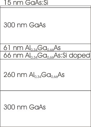
- The inverted HEMT device looks like this:
_________________________________________________________________
1
2 3
4
5 6
7 8
GaAs GaAs AlGaAs
AlGaAs:Si AlGaAs GaAs GaAs:Si
metal
200 nm 300
260 66
61 300
15 50
_________________________________________________________________
ohmic contact
- AlxGa1-xAs
We choose x to be 0.34.
In principle, we have a short-period lattice (SPS)
SPS GaAs/AlAs (2 nm / 1 nm)
but we consider it due to the short period to be stoichiometric equivalent to
Al0.34Ga0.66As which should simplify our calculations.
It improves the thermic resistence of the structures which underly a thermic
annealing step for activation of the doping materials.
- The flow scheme is 2:
1. calculate nonlinear Poisson as specified in input
For this example, we don't calculate the current.
- Output
- The band structure will be saved into the directory band_structure/
- The densities will be saved into densities/
- The strain will be saved into strain1/
- We are interested in plotting conduction band 1 and the resulting electron
density to visualize the two 2DEGs (two dimensional electron gas) which should
look somewhat like this:
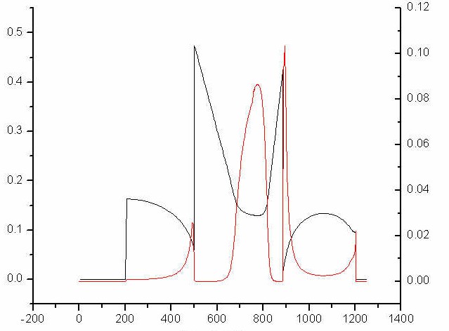
The
black curve shows conduction band 1 and the red curve shows the electron density. Clearly, one can see that
there are two triangular "bags" in the conduction band at GaAs/AlGaAs
interfaces. If these bags lie below the Fermi energy, 2DEGs (two dimensional
electron gases) can be formed. By variation of the doping concentration one
should be able to generate zero, one or two 2DEGs. By increasing the doping
concentration one should observe an increase in the number of electrons in the
left GaAs/AlGaAs interface, which is not desired. The task is to avoid this
and to get an 2DEG on the right side by choosing an appropriate doping profile.
- The 15 nm GaAs layer is doped with a constant n-type Si doping (2.0*1018
cm-3). The donor level of Si in GaAs lies 5.8 meV below the
conduction band.
$doping-function


 doping-function-number = 2             !
acts as separator
 impurity-number        =
  1             !
!
 doping-concentration   = 2.0           ! 2.0*10^18 cm^-3

 only-region            =
  1187.0 1202.0 !
  $end_doping-function


  $impurity-parameters


 impurity-number             =
  2
  !
 impurity-name               =
  Si-in-GaAs
  !
 impurity-type               =
  n-type
  ! n-type, p-type,
  trap

 number-of-energy-levels     = 1          !
 energy-levels-relative      =
  0.0058     !
! (n-type -> )
! Si in GaAs: 5.8 meV below conduction band
degeneracy-of-energy-levels = 2 ! 2 for n-type,
4 for p-type)
$end_impurity-parameters
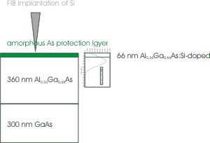
- The interior doping looks like this.
Experimental details: Si is implanted by FIB (focused ion beam) on an
amorphous As layer which will be removed after the implantation process.
$doping-function


 doping-function-number     = 1

 impurity-number            =
  1

 base-function-1            =
  gauss-1d                       !
a valid base function name
 apply-function-1-along-dir = 0 0 1                          ! (0 0 1) , (0 1 0) , (1 0 0)

 parameters-base-function-1 = 792.677  71.064   0.0   16.955 !
 doping-concentration       =
  1.5                            !
 only-region                =
  672.0 822.0

 position                   =
  792.677


  $end_doping-function


  $impurity-parameters


 impurity-number             =
  1

 impurity-name               =
  Si-in-GaAs

 impurity-type               =
  n-type

 number-of-energy-levels     = 1

 energy-levels-relativ       =
  0.0058

 degeneracy-of-energy-levels = 2


  $end_impurity-parameters
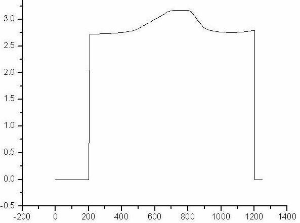
- A plot of the electrostatic potential looks like this:
|