nextnano3 - Tutorial
next generation 3D nano device simulator
1D Tutorial
HEMT structure (High Electron Mobility Transistor)
Authors:
Stefan Birner
->
  HEMT_1D_nn3.in / *_nnp.in -
input file for the nextnano3 and nextnano++ software
(1D simulation)
-> HEMT_2D_nn3.in

-> HEMT_3D_nn3.in
These input files are included in the latest version.
HEMT structure
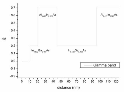
- This input file simulates a HEMT structure:
HEMT_1D_nn3.in
- It consists of:
at 10 nm: Schottky barrier of 0.2 eV
10 - 20 nm: In0.532Ga0.468As
20 - 45 nm: Al0.477In0.523As
45 - 95 nm: In0.532Ga0.468As
95 - ... nm: Al0.477In0.523As
The structure is grown on InP. There is no strain as everything is lattice
matched. (Nevertheless, we still calculate the strain.)
- Now we add at x = 35 nm a silicon delta doping of 4.5 * 1012 cm-2
which leads to band bending.
Instead of choosing a delta doping we specify a constant doping of 1.5 * 1020
cm-3 that extends over 0.3 nm.
(1.5 * 1020 cm-3 * 3 * 10-8 cm = 4.5 * 1012
cm-2)
$doping-function

   ...

  $end_doping-function


  $impurity-parameters

   ...

  $end_impurity-parameters
We obtain two eigenstates
and their corresponding wave functions
inside the HEMT channel which leads
to a two-dimensional electron gas (2DEG). The
electron density is plotted in blue.
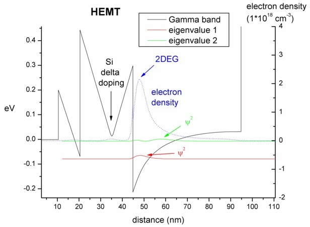
- In the file
densities/int_el_dens1D.dat we can find
the integrated density in each region cluster.
The total integrated density (from 10 nm to 100 nm) which can be measured
experimentally is thus
2.19 * 1012 cm-2 in agreement with the experiment. Most
of the density is located between 45 nm and 95 nm, namely 2.05 * 1012
cm-2.
2D/3D simulations
-> HEMT_2D_nn3.in

-> HEMT_3D_nn3.in
Input files for the same HEMT structure as in 1D, but this time for a
2D and 3D simulation are also available.
==> 2D: rectangle of dimension 250 nm x 10 nm
==> 3D: cuboid of dimension 250 nm x 10 nm x
10 nm
|