www.nextnano.com/documentation/tools/nextnano3/tutorials/1D_Mobility_2DEGs.html
nextnano3 - Tutorial
next generation 3D nano device simulator
1D Tutorial
Mobility in two-dimensional electron gases (2DEGs)
Authors:
Stefan Birner
If you want to obtain the input files that are used within this tutorial, please
check if you can find them in the installation directory.
If you cannot find them, please submit a
Support Ticket.
-> 1DInSb_mobility_ShaoFig3.in


-> 1DGaAs_mobility_WalukiewiczFig2.in

-> 1DGaAs_mobility_WalukiewiczFig3.in


-> 1DInGaAs_mobility_WalukiewiczFig8.in


-> 1DGaN_mobility_WalukiewiczFig4.in

-> 1DGaN_mobility_WalukiewiczFig5.in
Mobility in two-dimensional electron gases (2DEGs)
-> 1DInSb_mobility_ShaoFig3.in
This tutorial is based on the following paper:
[Shao]
Carrier Mobilities in delta-doped Heterostructures
Y. Shao, S.A. Solin, L.R. Ram-Mohan
(2006)
arXiv:cond-mat/0602140
Our implementation is based on the equations that are given in this paper
(with the exception of Eq. (3.5) where we added a factor of 1 / (4 pi) because
of SI units).
We calculate the mobility in a 40 nm InSb quantum well that is surrounded by
and strained with respect to Al0.15In0.85Sb barriers.
At z = -20 nm, there is a delta-doping layer with a sheet doping
density of 1 * 1012 cm-2.
The delta-doping layer is separated from the InSb QW by a 40 nm Al0.15In0.85Sb
spacer layer.
 quantum-well-width          =
40.0 ! [nm]    [Shao] Fig. 3

 spacer-width
= 40.0 ! [nm]    [Shao] Fig. 3

 remote-doping-sheet-density = 1e12 ! [cm^-2]
[Shao] Fig. 3
We calculate all properties for different temperatures. This can be done as
follows:
 $global-parameters

  lattice-temperature
= 1.0 ! T =
1 [K]
temperature-sweep-active
= yes ! 'yes'
/ 'no'
temperature-sweep-step-size =
10.0 ! increase temperature each time
by T = 10 [K]
temperature-sweep-number-of-steps = 31
! increase temperature 31 times
  data-out-every-nth-step
= 1     !
$end_global-parameters
.../..._ind000....dat
Here, the index runs from 0 (000) to 30 (030), i.e.
31 output files for each property in total.
We note that band gaps and lattice constants depend on temperature. This is
taken into account automatically for each temperature sweep.
The following figure shows the conduction band edge, the Fermi level and the
square of the lowest two electron wave functions at T = 1 K.
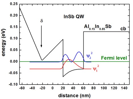
To plot such a figure, the following output files are needed:
- band_structure/cb1D_001_ind000.dat:
1st column: distance [nm]
2nd column: conduction band edge at the Gamma
point [eV]
Note: The index 'ind000' refers to the temperature
sweep. Here, index 0 means T = 1 K.
- current/fermi1Del_ind000.dat:
[nm]
2nd column: Fermi level of the electrons [eV]
In this tutorial, the Fermi level is always equal to 0 eV.
- Schroedinger_1band/cb001_ind000_sg1_deg1.dat:
[nm]
n columns: n energies of the eigenstates
[eV]
n columns: n squares of the wave functions (psi2)
[eV]
In the figure, we plotted the columns for psi2 of the
two lowest states: psi12,
psi22
The following figure shows the sheet electron density as a function of
temperature.
We considered the two lowest subbands for calculating the 2DEG density (the spin
degeneracy of the subbands is included):
2DEG-sheet-density-number-of-subbands = 2
Our results differ from the results of Fig. 3(b) of the [Shao] paper.
(Some obvious discrepancies are the conduction band offset (We used ~0.15 eV
whereas [Shao] used ~0.25 eV.) and the Schottky barrier height.)
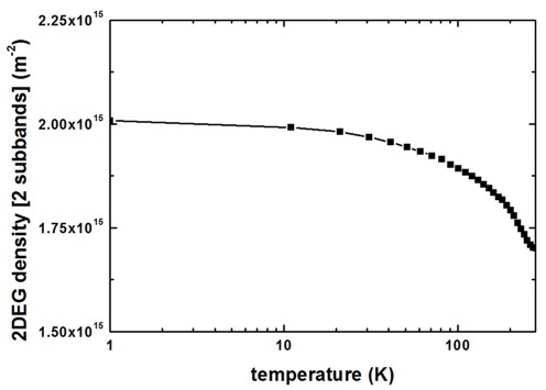
To plot such a figure, the following output file was used:
- Monte_Carlo/mobility_TemperatureSweep.dat:
1st column: temperature [K]
last column: electron sheet density of the lowest
subband(s) [m-2]
The following figure shows the calculated 2DEG mobility as a function of
temperature.
The relevant data can be found in this file:
- Monte_Carlo/mobility_TemperatureSweep.dat:
1st column: temperature [K]
2nd column: total mobility [m2/Vs]
3rd column: mobility due to ionized
impurity scattering [m2/Vs]
4th column: mobility due to background
impurity scattering [m2/Vs]
5th column: mobility due to deformation
potential acoustic phonon scattering [m2/Vs]
6th column: mobility due to polar optic
(LO)
phonon scattering [m2/Vs]
We included the following scattering mechanisms:
 ionized-impurity-scattering     =
yes ! [Shao]
(including remote and
background ionized impurity scattering)
 acoustic-phonon-scattering      =
yes ! [Shao]

 polar-optical-phonon-scattering = yes !
[Shao]
 alloy-scattering
= no  ! [Shao]
We now discuss the agreement/disagreement compared to Fig. 3(a) of the [Shao]
paper.
- The mobility due to acoustic phonon scattering is in excellent
agreement.
- The mobility due to polar optic LO phonon scattering is in
excellent agreement if one takes into
account that [Shao] forgot to include the factor of 1/(4 pi)
due to SI units.
- The mobility due to ionized and background impurity scattering
differs significantly.
It seems that the disagreement is not only due to the
different sheet density that has been used.
We used the following value:
  impurity-background-doping-concentration =
5e15 ! [cm^-3] [Shao] Fig. 3
The following InSb material parameters have been used:
 conduction-band-masses
= 0.0135   0.0135   0.0135   ! [m0] [Shao]


...
!
 static-dielectric-constants    =
16.82    16.82    16.82    ! [Shao]
epsilon(0)

 optical-dielectric-constants   =
15.7
! [Shao] epsilon(infinity)

 LO-phonon-energy
= 0.025
! [eV] [Shao] (optical phonon energy)


 mass-density
= 5.79e3
! [kg/m^3]  [Shao]

 sound-velocity
= 3.7e3
! [m/s]     [Shao]

 acoustic-deformation-potential = 7.2
! [eV]      [Shao]
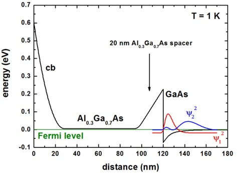
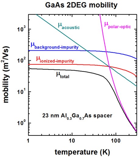
-> 1DGaAs_mobility_WalukiewiczFig2.in - (Experiment of Hiyamizu
et al.)
-> 1DGaAs_mobility_WalukiewiczFig3.in -
Here, we test our algorithm to results on GaAs 2DEGs of another publication.
We note that our algorithm is suitable for delta-doped 2DEGs but the GaAs
examples are not delta-doped.
This tutorial is based on the following paper:
[Walukiewicz]
Electron mobility in modulation-doped heterostructures
W. Walukiewicz, H.E. Ruda, J. Lagowski, H.C. Gatos
Physical Review B 30, 4571 (1984)
The experimental data is based on:
[Walukiewicz, Fig. 2]: [Hiyamizu]
Improved Electron Mobility Higher than 10^6
cm^2/Vs in Selectively Doped GaAs/N-AlGaAs Heterostructures grown by MBE
S. Hiyamizu, J. Saito, K. Nanbu
Japan. J. Appl. Phys. 22, L609 (1983)
[Walukiewicz, Fig. 3]: [DiLorenzo]
Material and device considerations for
selectively doped heterojunction transistors
J.V. DiLorenzo, R. Dingle, M. Feuer, A.C.
Gossard, R. Hendel, J.C.M. Hwang, A. Kastalsky, V.G. Keramidas, R.A. Kiehl,
P. O'Connor
IEEE-IEDM (International Electron Devices Meeting) 28,
578 (1982)
| [Walukiewicz, Fig. 2]: [Hiyamizu] |
|
[Walukiewicz, Fig. 3]: [DiLorenzo] |
| |
|
|
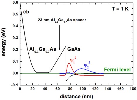
| Conduction band profile and
wave functions |
|
Conduction band profile and
wave functions |
|
20 nm Al0.3Ga0.7As
spacer
spacer-width = 20.0   ! 20
[nm] |
|
23 nm Al0.3Ga0.7As
spacer
spacer-width = 23.0   ! 23
[nm] |
 |
|
 |
| |
|
|
| |
|
|
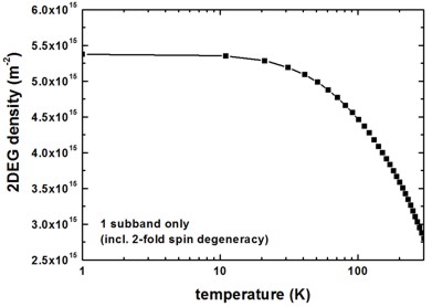
| 2DEG sheet density |
|
2DEG sheet density |
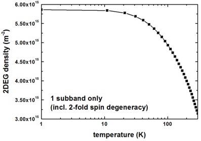 |
|
 |
| |
|
|
| |
|
|
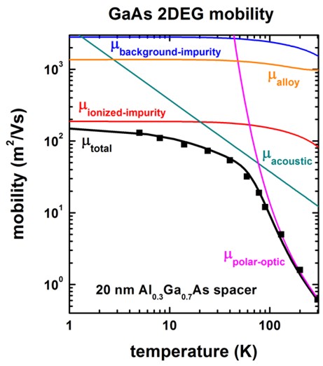
| Mobility |
|
Mobility |
|
		 impurity-background-doping-concentration = 9e13
		! [cm-3]

		 remote-doping-sheet-density       =
		3.5e11      ! [cm-2]
(to fit experiment)
		(remote-doping-sheet-density       =
		1.948344e11 ! [cm-2])
==> 8.6 * 1016 [cm-3]2/3
		=
		1.948344e11 (?)
|
|
		impurity-background-doping-concentration = 1e15
		! [cm-3]

		remote-doping-sheet-density
		= 1e12 ! [cm-2]
|
 |
|
 |
| |
|
|
| |
|
|
| Differences with respect to
Walukiewicz paper |
|
Differences with respect to
Walukiewicz paper |
|
|
|
In Walukiewicz's paper, the
background impurity scattering is
dominating the ionized impurity scattering.
We found the opposite. |
| |
|
|
|
Walukiewicz used a 2DEG density of 3 * 1011
cm-2. |
|
Walukiewicz used a 2DEG density of 2.2 -
3.8 * 1011 cm-2. |
|
conduction-band-masses = 0.067   0.067   0.067   ! [m0]


...
!
a higher value than for bulk because of nonparabolicity
Here we used 0.067 as this gives better
agreement to the mobility at higher temperatures and
this is the usually accepted material parameter for GaAs
quantum-well-width = 13.0 ! [nm] (13
nm seems to be a better value than 20 nm.)
alloy-scattering   =
		yes
Alloy scattering is relevant for the part of the wave function that
penetrates into the AlGaAs barrier.
The
squares are experimental values of Fig. 5 in:
Improved Electron Mobility Higher than 106 cm2/Vs
in Selectively Doped GaAs/N-AlGaAs Heterostructures Grown by MBE
S. Hiyamizu et al.
Jpn. J. Appl. Phys. 22, L609 (1983) |
|
conduction-band-masses = 0.076   0.076   0.076   ! [m0] [Walukiewicz]


...
!
a higher value than for bulk because of nonparabolicity. This is also
the value used by Walukiewicz.
quantum-well-width = 20.0 ! [nm] (This
value might be too large. See left where 13 nm was used.)
alloy-scattering   =
		no
|
The following GaAs material parameters have been used:
 static-dielectric-constants    =
12.9    12.9    12.9    !
[Walukiewicz] epsilon(0)

 optical-dielectric-constants   =
10.9
! [Walukiewicz] epsilon(infinity)

 LO-phonon-energy
= 0.036
! [eV] [Walukiewicz] (optical phonon energy)


 mass-density
= 5.318e3
! [kg/m^3]  [Davies] p. 411

 sound-velocity
= 5.29e3
! [m/s]     [X.L. Lei, J. Phys. C 18, L593 (1985)]

 acoustic-deformation-potential = 7.0
! [eV]      [Walukiewicz]
Into the equation for the deformation potential
acoustic phonon scattering, the quantum well width is an input
parameter.
We used a value of 13 nm which corresponds roughly to the extension of the
ground state wave function inside the "triangular" QW.
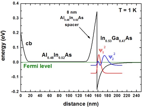
-> 1DInGaAs_mobility_WalukiewiczFig8.in - (Experiment of Kastalsky
et al.)
Here, we test our algorithm to results on InGaAs 2DEGs of another
publication.
We note that our algorithm is suitable for delta-doped 2DEGs but the
InGaAs examples are not delta-doped.
This tutorial is based on the following paper:
[Walukiewicz]
Electron mobility in modulation-doped heterostructures
W. Walukiewicz, H.E. Ruda, J. Lagowski, H.C. Gatos
Physical Review B 30, 4571 (1984)
The experimental data is based on:
[Walukiewicz, Fig. 8]: [Kastalsky]
Two-dimensional electron gas at a molecular beam
epitaxial-grown, selectively doped, In0.53Ga0.47As-In0.48Al0.52As
interface
A. Kastalsky, R. Dingle, K.Y. Cheng, A.Y. Cho
Applied Physics Letters 41, 274 (1982)
[Kastalsky] and [Walukiewicz] have used In0.48Al0.52As
whereas we used In0.52Al0.48As
which is lattice matched to InP and In0.53Ga0.47As.
The conduction band profile is shown in the following figure.
Here, two subbands (psi12,
psi22) are occupied
although our implementation of calculating the mobility is only applicable to
one occupied subband.
Note that the 2DEG is located in an alloy, i.e. InGaAs. Thus we expect that
alloy scattering has a significant effect on the total mobility.
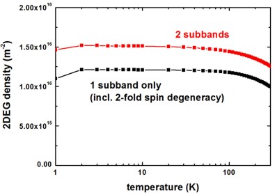
The following figure shows the subband density of the first subband
and of the first two subbands as a function
of temperature.
Inside the mobility algorithm, only the density of the first subband has been
considered.
The following figure shows the mobility as a function of temperature.
At temperatures below 100 K, the total mobility is dominated by alloy
scattering.
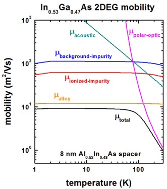
Our results for the mobility are in reasonable agreement with Fig. 8 of the
paper of [Walukiewicz].
The following parameters have been used:
 ionized-impurity-scattering
= yes     !
(including
remote and background ionized impurity scattering)
 acoustic-phonon-scattering
= yes     !

 polar-optical-phonon-scattering
= yes     !
 alloy-scattering
= yes     !
 quantum-well-width
= 15.0    ! [nm]
15 nm seems
to be a reasonable approximation for the triangular well
 spacer-width
= 8.0     ! [nm]

 impurity-background-doping-concentration = 1.0e16
! [cm-3]

 remote-doping-sheet-density
= 1.0e12  ! [cm-2]

 2DEG-sheet-density-number-of-subbands    =
1

 alloy-disorder-scattering-potential      =
0.60    ! [eV]
InGaAs bulk value [J.R.
Hayes et al. (1982)]
!----------------------------------------------------------------------------

! In0.53Ga0.47As material parameters

!----------------------------------------------------------------------------

 mass-density
= 5.5025e3  ! [kg/m^3] InGaAs
 sound-velocity
= 4.753e3   ! [m/s]    In0.53Ga0.47As[111]
[Wen et al., JAP 100, 103516 (2006)]
 acoustic-deformation-potential = 7.0
 ! [eV]     InGaAs
[Walukiewicz]
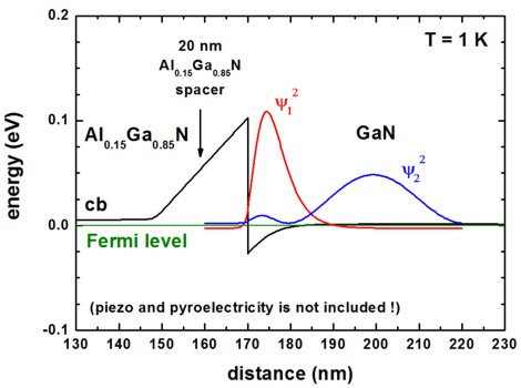
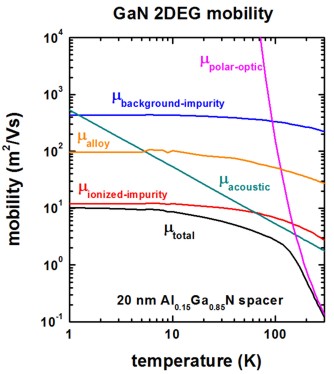
-> 1DGaN_mobility_WalukiewiczFig4.in
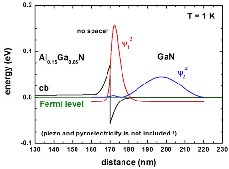
-> 1DGaN_mobility_WalukiewiczFig5.in
Here, we test our algorithm to results on GaN 2DEGs of another publication.
We note that our algorithm is suitable for delta-doped 2DEGs but the GaN
examples are not delta-doped.
This tutorial is based on the following paper:
[WalukiewiczGaN]
Electron mobility in AlxGa1-xN/GaN heterostructures
L. Hsu, W. Walukiewicz
Physical Review B 56, 1520 (1997)
Note: To be consistent with the paper of Walukiewicz, no (!) piezo- and
pyroelectricity is included.
| [WalukiewiczGaN] Fig. 4 |
|
[WalukiewiczGaN] Fig. 5 |
| |
|
|
| Conduction band profile and
wave functions |
|
Conduction band profile and
wave functions |
|
20 nm Al0.15Ga0.85N
spacer
spacer-width = 20.0   ! 20
[nm] |
|
no spacer
spacer-width = 0.0   ! 0
[nm] |
| |
|
|
 |
|
 |
Into the equation for the
deformation potential acoustic phonon scattering, the quantum
well width is an input parameter.
We used values which correspond roughly to the extension of the ground
state wave function inside the "triangular" QW. |
quantum-well-width = 15.0 ! 15
[nm] |
|
quantum-well-width = 10.0 ! 10
[nm] |
| |
|
|
| |
|
|
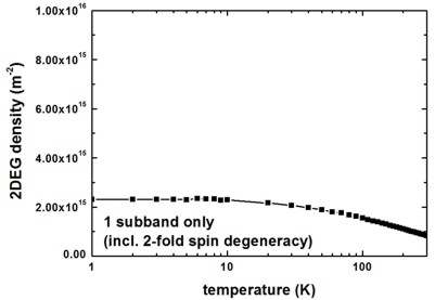
| 2DEG sheet density |
|
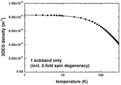
2DEG sheet density |
 |
|
 |
|
[WalukiewiczGaN] used a 2DEG density of
6.2 * 1015 m-2. |
|
[WalukiewiczGaN] used a 2DEG density of
1.59 * 1016 m-2. |
| |
|
|
| |
|
|
| Mobility |
|
Mobility |
|
		impurity-background-doping-concentration = 1e14
		! [cm-3]

		remote-doping-sheet-density       =
		7.883735e11 ! [cm-2]
[WalukiewiczGaN] Fig. 4: 7 * 1017 [cm-3]
==> 7 * 1017 [cm-3]2/3
|
|
		impurity-background-doping-concentration = 4e15
		! [cm-3]

		remote-doping-sheet-density
		= 1e12 ! [cm-2]
|
 |
|
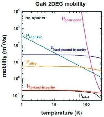 |
		alloy-disorder-scattering-potential = 2.3
		! [eV]
conduction band offset GaN/AlN |
The following GaN material parameters have been used:
 conduction-band-masses
= 0.21     0.21     0.21       ! [m0]
[WalukiewiczGaN]

 static-dielectric-constants    =
9.5      9.5      9.5        ! [WalukiewiczGaN]
epsilon(0)

 optical-dielectric-constants   =
5.35
5.35
 5.35
! [WalukiewiczGaN] epsilon(infinity)

 LO-phonon-energy
= 0.0905   0.0905   0.0905
! [eV] [WalukiewiczGaN] (optical phonon energy)


 mass-density
= 6.1e3
! [kg/m^3]  [WalukiewiczGaN]

 sound-velocity
= 6.6e3                        ! [m/s]     [WalukiewiczGaN]

 acoustic-deformation-potential = 8.5                          ! [eV]      [WalukiewiczGaN]
Here, alloy scattering is only relevant for the part of the wave function that
penetrates into the AlGaN barrier.
Final remark: In principle, the results of these GaN 2DEGs are not reliable
as piezo- and pyroelectricity have to be included.
Our results disagree quantitatively with the results of [WalukiewiczGaN].
However, it is not clear, which material parametes he used for the conduction
band offset and the alloy scattering.
Further hints
If two remote doping regions should be taken into account, one can input an
array of values.
spacer-width
= 20.0   10.0   ! [nm]
remote-doping-sheet-density           = 1e12
1e11
! [cm-2]
|