|
| |
nextnano3 - Tutorial
next generation 3D nano device simulator
1D Tutorial
p-Si / SiO2 / poly-Si structure (MOSFET with inversion channel
due to applied gate voltage)
Authors:
Stefan Birner
If you want to obtain the input file that is used within this tutorial, please
submit a support ticket.
-> 1DpSi_SiO2_npolySi_Gate.in
p-Si / SiO2 / poly-Si structure (MOSFET with inversion channel
due to applied gate voltage)
Step 1: Layer sequence
| # |
width [nm] |
material |
doping |
|
| 1 |
1 |
contact |
|
|
| 2 |
99 |
p-Si |
5 x 1017 cm-3 (fully ionized) |
|
| 3 |
5 |
SiO2 |
|
|
| 4 |
54 |
n-Si (poly-silicon) |
3 x 1019 cm-3 (fully ionized) |
|
| 5 |
1 |
Gate contact |
|
|
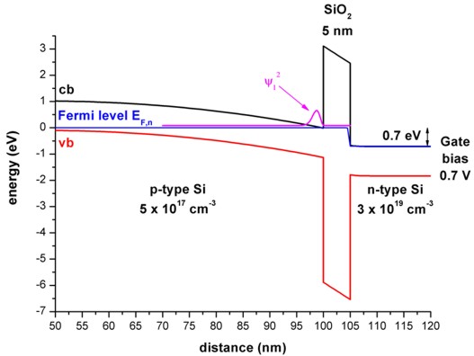
The applied gate voltage leads to confined electron states at the p-Si / SiO2
interface (n-type inversion layer) whereas the holes are repelled from
the Si/SiO2 surface towards the interior of the device (i.e. to the
left side).
An applied source-drain voltage in the plane of the inversion layer will lead to
a flow of current which depends on the sheet density in the inversion layer.
The magnitude of the current is governed by applied gate voltage, i.e. the gate
controls the sheet density and thus switches the current on or off (MOSFET,
metal-oxide-semiconductor field effect transistor).
Step 2: Calculations
The temperature was set to 300 Kelvin.
Self-consistent solution of the 1D-Schrödinger-Poisson equation within single-band
effective-mass approximation (using ellipsoidal effective mass tensors) for the
(Delta) conduction band edges.
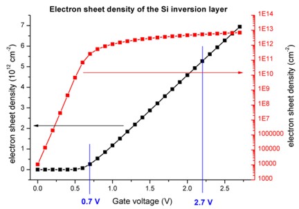
We vary the gate voltage from 0 V to 2.7 V in steps of 0.1 eV.
Step 3: Results
- The following two figures show the band profiles and the electron density
for two different gate voltages:
a) 0.7 V (The electron ground state is above the electron Fermi level.)
b) 2.7 V (The electron ground state is below the electron Fermi level
and thus occupied, leading to a large quantum mechanical density.)
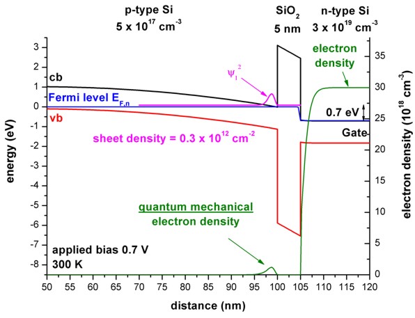
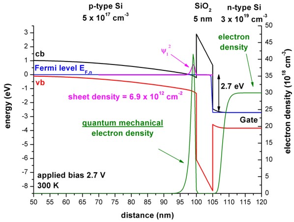
In the poly-silicon on the right side of the SiO2 barrier, the
electrons get depleted from the oxide interface.
Due to the fact that the Fermi level is
constant outside the SiO2 barrier, no current is flowing.
(Inside the SiO2 barrier the Fermi level has a step-like feature.
But as the electron density is zero inside the barrier, no current is
flowing.)
The ground state electron level is associated with the longitudinal electron
mass (mlongitudinal = 0.916 m0)
whereas the second and the third eigenstate (which are degenerate) are
associated with the transversal electron mass (mtransversal = 0.190 m0).
Due to this degeneracy, only two rather than three Schrödinger
equations have to be solved:
a) V(z), mzz = mtransversal = 0.190 m0
b) V(z), mzz = mlongitudinal = 0.916 m0
The potential V(z) that enters into the Schrödinger equation is the same
in these two cases.
ev1D_cb003_ind0**_qc001_sg001_deg001_neu_Kx001_Ky001_Kz001.dat
The eigenvalues for mlongitudinal are contained in:
ev1D_cb003_ind0**_qc001_sg001_deg002_neu_Kx001_Ky001_Kz001.dat
At 2.5 eV the energy spacing between the two lowest electron states is of the order 100
meV (in the case of longitudinal effective mass).
At 2.5 eV the energy spacing between the two lowest electron states is of the order 130
meV (in the case of transversal effective mass).
At 2.5 eV the energy spacing between the electron ground state (with longitudinal
effective mass) and the ground state of the tranversal effective mass is of
the order 80 meV. Thus, in this case one can safely assume that only one electron state is
occupied, i.e. the electron ground state with the longitudinal mass.
- Electron sheet density in the inversion channel as a function of
applied gate voltage
The file densities/int_el_dens1D.dat contains the integrated
electron density for each region cluster.
The p-Si region, where the inversion channel is located, is termed "region
cluster 2" and extends from 1 nm to 100 nm.
To plot the integrated electron charge density of the p-Si region vs. gate
voltage, one has to plot the second column of this file.
To obtain the capacitance-voltage characteristics, one has to calculate the
derivative of this column.
|