|
| |
nextnano3 - Tutorial
next generation 3D nano device simulator
1D Tutorial
Optical absorption of an InGaAs quantum well
Author:
Stefan Birner
If you want to obtain the input files that are used within this tutorial, please
check if you can find them in the installation directory.
If you cannot find them, please submit a
Support Ticket.
-> InGaAs_7nm_optics_step1.in
   InGaAs_7nm_optics_step2.in


    InGaAs_7nm_optics_step3_x_polarized.in


    InGaAs_7nm_optics_step3_z_polarized.in
InGaAs quantum well
- We want to calculate the optical absorption as a function of photon energy
for interband (i.e. electron-hole) transitions in a quantum well by means of
8-band k.p theory.
- This input file simulates a 7 nm In0.3Ga0.7As
quantum well embedded in GaAs which acts as the barrier material. The InGaAs
quantum well is strained pseudomorphically with respect to the substrate
material GaAs (001). The temperature is assumed to be 150 K. The effect of
strain is included into the 8-band k.p Hamiltonian.
- Detailed description about the physical background that is used to
calculate the optical absorption:
Absorption, Matrix elements, Inter-band transitions, Intra-band transitions
(pdf file).
Restrictions: The physical model is only correct for [001] growth direction.
We also neglect the k vector dependence of the matrix elements.
- The
$numeric-control features that have to be used are:
$numeric-control

   simulation-dimension = 1

 ...

  $end_numeric-control
To calculate the optical absorption, we have to perform a 3-step approach:
- Step 1: Here: Calculate k.p eigenstates for k||=0
calculate-optics = no
Solve k.p and determine lowest and highest eigenvalue to specify
e-min-state and e-max-state in the second step.
Note: Usually one could do the following:
- Solve for self-consistent potential with effective-mass approximation
instead of 8-band k.p. This is much faster.
- Write out raw data for potential and Fermi levels (and strain if necessary).
- Use this potential and these Fermi levels to solve 8-band k.p
eigenstates in step 2.
- Step 2: Calculate eigenstates for k||/=0
  calculate-optics = yes

  read-in-k-points = no
raw-potential-in = yes, raw-fermi-levels-in
	= yes, strain-calculation =
  raw-strain-in
- Step 3: Calculate optical absorption
  calculate-optics = yes

  read-in-k-points = yes
If one wants to repeat the calculation for another polarization, one only
needs to change the polarization vector and repeat step 3.
It is not necessary in this case to recalculate step 1 or step 2.
Step 1: Calculate k.p eigenstates for k||=0
- For step 1, the relevant specifier for the keyword
$optical-absorption is only the following:
 calculate-optics      =
  no
This is equivalent to not including this keyword at all. For
step 1 we do not need optics, we just calculate the k.p eigenstates.
  $optical-absorption

 destination-directory = optics1/
  !
 calculate-optics      = no
! yes"/"no"
 kind-of-absorption    =
interband-only ! 'interband-only''intra-vb-only', 'intra-cb-only'
read-in-k-points = no
! flag: "yes"/"no"
 ...


  $end_optical-absorption
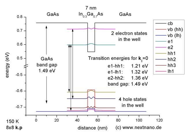
- This pictures shows the calculated electron and hole states that are bound
inside the well. The conduction (cb) and valence band edges (hh: heavy hole,
lh: light hole) are also indicated. The electron and hole states that are not
bound inside the well are not shown although they are needed to calculate the
optical absorption.
The transition energies that are relevant
for the interband (i.e. electron-hole) transitions were calculated. Note that
'lh1' corresponds to the first light hole state, and hh1, hh2 and hh3 to the
heavy holes. These transition energies between bound states were calculated
without taking into account the exciton corrections. The three lines indicate
the strongest transitions: The "Delta n = 0" selection rule, i.e. transitions
between levels with the same index.
Figure 1:
Step 2: Calculate eigenstates for k||/=0
- For step 2, the relevant specifiers for the keyword
$optical-absorption are the following:
In step 1 we used:
 calculate-optics      =
  no
This time we need:
 calculate-optics      =
  yes
  $optical-absorption

 destination-directory = optics1/
  !
 calculate-optics      = yes
! yes"/"no"
 kind-of-absorption    =
interband-only ! 'interband-only' (8x8kp)'intra-cb-only'
(8x8kp),
'intra-vb-only' (6x6kp)

 read-in-k-points      = no
  !
flag: "yes"/"no"
  !

                                        !
 e-min-state
  = -0.80d0
  !
 e-max-state           =
  1.60d0
  !
 ...


  $end_optical-absorption
read-in-k-points = no,
we therefore have to specify the relevant parameters that are needed for the k
point calculations.
$quantum-model-electrons
 ...

 num-kp-parallel  =
  1000   ! STEP 2/3
  !
total number of k|| points for Brillouin zone
discretization
$quantum-model-holes
 ...

 num-kp-parallel  =
  1000   ! STEP 2/3
  !
total number of k|| points for Brillouin zone
discretization
- Explanations:
- In order to study interband (electron-hole) transitions, we need 8-band k.p.
- From Figure 1 we obtain the minimum and maxium
energy of the eigenstates that will be considered for transitions. We consider
all electron states up to 1.6 eV and all hole states up to -0.8 eV (CHECK: It
seems that -0.8 is not low enough). This corresponds to 50 eigenvalues for the
electrons and 40 for the holes.
- Output
Once the calculation of step 2 is done, the folder optics1/
contains the following files:
optics_out_eigenvalues_el1D.txt - contains electron
eigenvalues
in ASCII format
optics_out_eigenvalues_hl1D.txt -
optics_out_spinor_el1D.raw -
optics_out_spinor_hl1D.raw -
They contain for each k|| = (kx,ky)
value, the k.p wave function components (spinors) for all eigenvalues.
In detail:
- We have 95 grid points in the quantum region (from 30 nm to
77 nm), i.e. a grid point resolution of 0.5 nm which is rather coarse.
This means that each spinor has a size of 96.
grid = 95
- We have 8-band k.p, i.e. 8 spinors.
    spinor = 8

	-
The dimension of the matrix that we have to diagonalize for each
k|| point is 760, i.e. a 760 x 760 matrix.
grid * spinor = 95 * 8 = 760
- We have 961 k|| points, i.e. 961 matrices
have to be diagonalized.
    k_parallel = 961

	-
The wave functions are complex, thus we have to store two numbers, a
real part and an imaginary part.
    complex = 2


	==>
For each eigenvalue of a k|| point we have to
store the following amount of data for its wave function:
    complex * k_parallel * spinor * grid =

       2    *
	961    *   8    * 95   =
	1,460,720
 ==>
	11,685,760 byte = 11.14 MB


	-
However, there are several eigenvalues (and thus wave function
components (spinors) for each of them) for each k|| point
which have to be stored.
number of electron eigenvalues:
MAX_NUM_EL1D = 50
number of hole eigenvalues:
	MAX_NUM_HL1D = 38


    ==>
for electrons: 50 * 11.14 MB = 557.22 MB
(corresponding to the size of the file optics_out_spinor_el1D)
==> 38 * 11.14 MB =
423.49 MB (corresponding to the size of the file
optics_out_spinor_hl1D)
These data files will be read in in the next step (Step 3).
Step 3: Calculate optical absorption
- For step 3, the relevant specifiers for the keyword
$optical-absorption are the following:
In step 2 we used:
 calculate-optics            =
  yes

 read-in-k-points            =
  no
This time we need:
 calculate-optics            =
  yes
 read-in-k-points
  = yes


  $optical-absorption

 destination-directory       = optics1/
  !
directory for output and data files
 calculate-optics            =
  yes
! yes"/"no"
 kind-of-absorption          =
interband-only ! 'interband-only''intra-vb-only', 'intra-cb-only'
read-in-k-points =
yes
! flag: "yes"/"no"
	 e-min-state
  = -0.80d0
  !
 e-max-state
  =  1.60d0
  !
!
 e-min-photon                =
  1.10d0
  ! [eV]
 e-max-photon                =
  1.60d0
  ! [eV]
 smoothing-of-curve          =
	yes
!
 smoothing-damping-parameter =
  5d-4           ! [eV]
 num-energy-steps            =
  1000
  !
!
 polarization-vector-1       = 1d0 0d0 0d0
  !
 polarization-vector-2       = 0d0 1d0 0d0
  !
 magnitude-relation-1-2      = 0d0
! |E1|/|E2|
phase
= 0.0d0
! phase: E2 -> exp(i*phase*Pi)*E2
$end_optical-absorption
If read-in-k-points = yes,
we read in the data files that were created in step 2:
optics1/optics_out_eigenvalues_el1D

        optics_out_eigenvalues_hl1D

        optics_out_spinor_el1D

        optics_out_spinor_hl1D
- Figure 2 shows the optical absorption spectrum as a function of photon
energy for x- and z- polarized light.
x-polarized light (black line): The light propagation is normal to the
quantum well along the z direction. Here, it is x-polarized. If it were
y-polarized, the same absorption spectrum would have been obtained.
z-polarized light (red line): The light
propagation is in the plane of the quantum well with perpendicular E-field
polarization (along the z direction). This is the transverse magnetic (TM)
mode. No absorption for heavy holes is seen. (This is not exactly true
because the TM mode has a component of the electric field along the direction of
propagation x. But it is small in a weakly guiding structure.) Consequently in
Fig. 2 only the transition involving the light hole is seen (e1-lh1)
and the heavy hole transitions are suppressed (e1-hh1, e2-hh2).
Figure 2
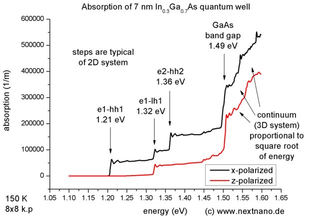
The optical absorption spectrum ranges from 1.10 eV to 1.60 eV. The relevant
specifiers to determine this range are:
 e-min-photon
  = 1.10d0
  !
lower boundary for photon energy interval
 e-max-photon           =
  1.60d0
  !
The energy interval from 1.10 eV to 1.60 eV ([e-min-photon,e-max-photon]
= [1.10d0,1.60d0])
is divided into a number of energy steps (energy grid) that must be specified in the input
file: num-energy-steps = 1000
How to specify x-polarized light:
 polarization-vector-1  = 0d0 1d0 0d0
  !
x y z coordinates (in simulation system) for first in-plane vector
 polarization-vector-2  = 1d0 0d0 0d0
  !
 magnitude-relation-1-2 = 0d0
! |E1|/|E2|
(In this case, polarization-vector-1 is ignored as
|E1| is set to be zero.)
 polarization-vector-1  = 1d0 0d0 0d0
  !
x y z coordinates (in simulation system) for first in-plane vector
 polarization-vector-2  = 0d0 0d0 1d0
  !
 magnitude-relation-1-2 = 0d0
! |E1|/|E2|
(In this case, polarization-vector-1 is ignored as
|E1| is set to be zero.)
 polarization-vector-1  = 1d0 0d0 0d0
  !
x y z coordinates (in simulation system) for first in-plane vector
 polarization-vector-2  = 0d0 0d0 1d0
  !
 magnitude-relation-1-2 = 1d0
! |E1|/|E2|
(In this case, polarization-vector-1 is not ignored as
|E1|=|E2|.)
Exciton binding energy in quantum wells
- In order to correlate the calculated optical transition energies of a 1D
quantum well to experimental data, one has to include the exciton
(electron-hole pair) corrections.
- GaAs band gap transition at 1.49 eV:
The 3D bulk exciton binding energy can be calculated analytically
Eex,b = - µ e4 / ( 32 pi² hbar² er²
e0²) = - µ / (m0 er²) x 13.61 eV
where µ is the reduced mass of the
electron-hole pair: 1/µ = 1/me + 1/ mh
hbar is Planck's constant
divided by 2pi
e is the electron charge
er is the dielectric constant
e0 is the vacuum permittivity
m0 is the rest mass of the
electron and
13.61 eV is the Rydberg energy.
In GaAs it is equal to -4.8 meV.
Thus the energy of the exciton, i.e. band gap transition, reads
Eex = Egap + Eex,b = 1.49 eV - 0.005 eV
= 1.485 eV.
A 1D quantum well for a type I structure has two exciton limits for the ground
state transition (e1-hh1):
- infinitely thin quantum well (2D limit): Eex,qw = 4Eex
- infinitely thick quantum well (3D bulk exciton limit): Eex,qw = Eex
Between these limits, the exciton correction which depends on the well
width has to be calculated numerically, not only for the ground state but also
for excited states (e.g. e2-hh2, e1-lh1).
For more details, please have a look at our 1D exciton tutorial:
Exciton energy in quantum wells
|