|
| |
nextnano3 - Tutorial
1D Tutorial
Double Quantum Well
Author:
Stefan Birner
-> DoubleQuantumWell_6_nm_nn3.in - input file for the nextnano3 software
DoubleQuantumWell_6_nm_nnp.in -
Double Quantum Well
This tutorial aims to reproduce two figures (Figs. 3.16, 3.17, p. 92) of
Paul Harrison's
excellent book "Quantum
Wells, Wires and Dots" (Section 3.9 "The Double Quantum Well"), thus the following description is based on the
explanations made therein.
We are grateful that the book comes along with a CD so that we were able to
look up the relevant material parameters and to check the results for
consistency.
Double Quantum Well: AlGaAs / 6 nm GaAs / 4 nm AlGaAs / 6 nm GaAs /
AlGaAs
- Our symmetric double quantum well consists of two 6 nm GaAs quantum wells,
separated by a 4 nm Al0.2Ga0.8As barrier and
surrounded by 20 nm Al0.2Ga0.8As barriers on each side.
We thus have the following layer sequence: 20 nm Al0.2Ga0.8As
/ 6 nm GaAs / 4 nm Al0.2Ga0.8As / 6 nm GaAs /
20 nm Al0.2Ga0.8As.
The barriers are printed in bold.
- This figure shows the conduction band edge and the lowest two electron
eigenenergies and wave functions that are
confined inside the wells.
(Note that the energies were shifted so that the conduction band edge of GaAs
equals 0 eV.)
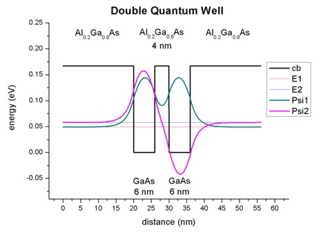
- The wave functions form a symmetric and an anti-symmetric pair. The
symmetric one is lower in energy than the anti-symmetric one.
The plot is in excellent agreement with Fig. 3.17 (page 92) of
Paul Harrison's
book "Quantum
Wells, Wires and Dots".
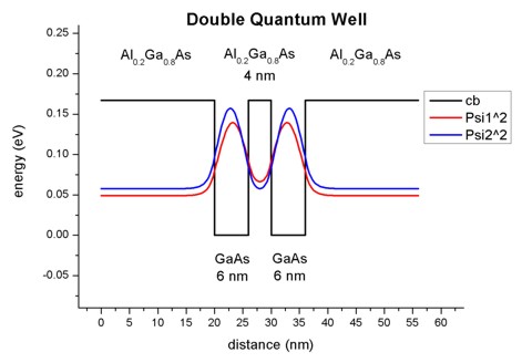
- For comparison, the following figure shows for the same structure as
above, the square of the wave function rather than Psi only.
- Output
a) The conduction band edge of the Gamma conduction band can be
found here:
band_structure / cb_Gamma.dat
b) This file contains the eigenenergies of the two lowest
eigenstates. The units are [eV].
Schroedinger_1band / ev_cb1_qc1_sg1_deg1.dat
  num_ev:  eigenvalue [eV]:


  1        0.04920


  2        0.05779
nextnano++:
  num_ev:  eigenvalue [eV]:


  1        0.04920


  2        0.05779
Paul Harrison's book: 1
0.04912
2 0.05770
c) This file contains the eigenenergies and the
squared wave functions (Psi²):
Schroedinger_1band / cb1_qc1_sg1_deg1_psi_squared_shift.dat
Schroedinger_1band / cb1_qc1_sg1_deg1_psi_shift.dat
_shift
indicates that Psi² and Psi are shifted by the corresponding energy
levels.
Double Quantum Well: AlGaAs / 6 nm GaAs / ... nm AlGaAs / 6 nm GaAs /
AlGaAs
- Here, we varied the thickness (from 1 nm to 14 nm) of the Al0.2Ga0.8As
barrier layer that separates the two quantum wells and calculated the energies
of the two lowest eigenstates. The width of the quantum wells is fixed (6 nm).
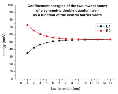
If the separation between the two quantum wells is large, the wells behave as
two independent single quantum wells having the identical ground state
energies. The interaction between the energy levels localized within each well
increases once the distance between the two wells decreases below 10 nm. One
state is forced to higher energies and the other to lower energies. Here, the
electron spins align in an "anti-parallel" arrangement in order to satisfy the
Pauli exclusion principle.
- This is analogous to the hydrogen molecule where the formation of a pair
of bonding and anti-bonding orbitals occurs once the two hydrogen atoms A and
B are brought together.
Psibonding
= 1/SQRT(2) ( PsiA + PsiB )
(lower energy)
Psianti-bonding = 1/SQRT(2)
( PsiA - PsiB )
(higher energy)
- Again, the plot is in excellent agreement with Fig. 3.16 (page 92) of
Paul Harrison's
book "Quantum
Wells, Wires and Dots".
- Output: The energy values were taken from this file:
Schroedinger_1band / ev_cb1_qc1_sg1_deg1.dat
  num_ev:  eigenvalue [eV]:


  1        0.03476


  2        0.07298
nextnano++:
  num_ev:  eigenvalue [eV]:


	1        0.03476


	2        0.07298
Paul Harrison's book: 1
0.03470
2 0.07290
The values for the 14 nm barrier read:
  num_ev:  eigenvalue [eV]:


	1        0.05332


  2        0.05338
nextnano++:
  num_ev:  eigenvalue [eV]:


	1        0.05332


	2        0.05338
Paul Harrison's book: 1
0.05323
2 0.05329
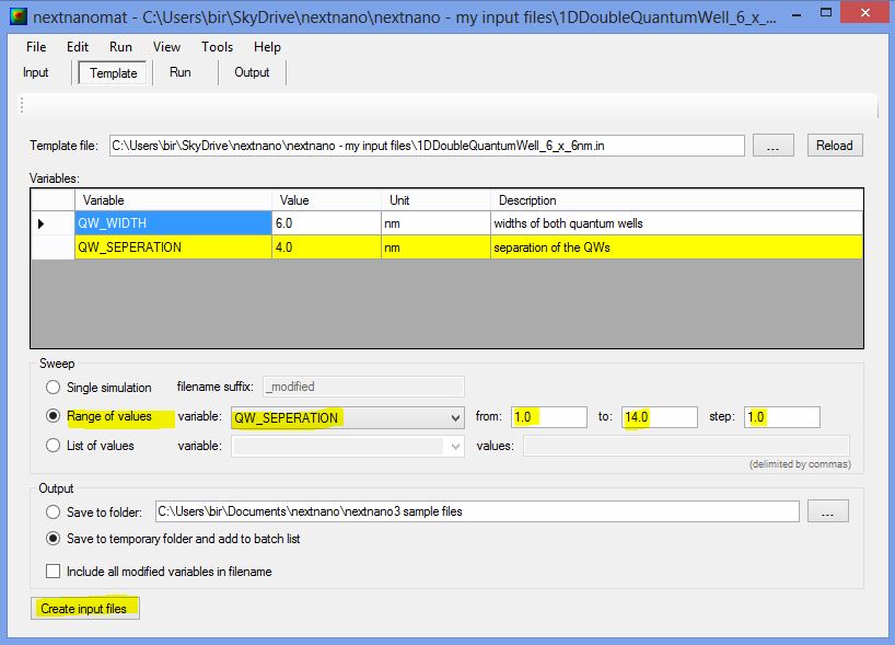
A sweep over the thickness of the Al0.2Ga0.8As
barrier layer, i.e. the variable %QW_SEPARATION, can be done
easily by using nextnanomat's
Template feature.
The following screenshot shows how this can be done.
Go to "Template", open input file, select "Range of values", select
"QW_SEPARATION", click on "Create input files", go to "Run and start your
simulations.
Another tutorial on coupled quantum wells can be found
here.
|