nextnano3 - Tutorial
next generation 3D nano device simulator
1D Tutorial
Capacitance-Voltage curve of a "metal"-insulator-semiconductor (MIS)
structure
Authors:
Stefan Birner
-> MIS_CV_1nmSiO2_1D_nn3.in / *_nnp.in - input file for the nextnano3
and nextnano++ software
MIS_CV_3nmSiO2_1D_nn3.in / *_nnp.in -
MIS_CV_3nmSiO2_metal_1D_nn3.in / *_nnp.in -
MIS_CV_3nmSiO2_metal_2D_nn3.in / *_nnp.in - input file for the nextnano3
and nextnano++ software
These input files are included in the latest version.
Capacitance-Voltage curve of a "metal"-insulator-semiconductor (MIS)
structure
In this tutorial we calculate the C-V (capacitance-voltage) characterstics of
a poly-Si / SiO2 / Si structure.
This tutorial is based on the following paper:
[Richter]
A Comparison of Quantum-Mechanical Capacitance-Voltage Simulators
C.A. Richter, A.R. Hefner, E.M. Vogel
IEEE Electron Device Letters 22 (1), 35 (2001)
Our structure consists of a heavily n-type doped poly-silicon (gate
material), a thin SiO2 layer (insulator), and a p-type doped Si
substrate.
Such a structure is similar to a MIS (metal-insulator-semiconductor) structure
(or MOS = metal-oxide-semiconductor).
We apply a voltage of VG = -3 V to the poly-Si region
and vary this voltage stepwise until VG = +3 V.
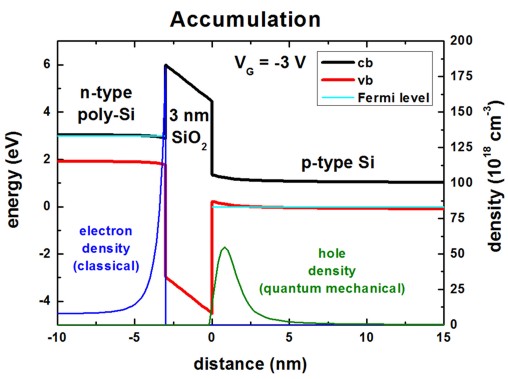
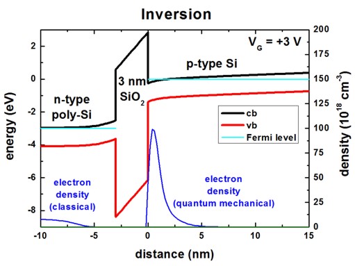
Accumulation and inversion
-> MIS_CV_3nmSiO2_1D_nn3.in / *_nnp.in
The following two figures show the band profiles and the electron and hole densities
for two different gate voltages:
The left figure shows the conduction (Delta (X) valley) and valence band edges
of this structure at VG = -3 V
where in the p-type Si region the charge density is dominated by holes (accumulation).
The right figure is for VG = +3 V where in the p-type Si region the
charge density is dominated by electrons (inversion).
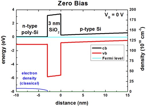
The band profile for zero bias is indicated here. Inside the quantum region
(0 nm - 50 nm), the electron and hole density in the p-type Si is essentially
zero.
From 50 nm to 200 nm the hole density is nonzero (0.21 * 1018 cm-3,
mostly heavy hole contribution).
The following parameters were used:
- SiO2 thickness: 3 nm
- doping concentration: p-type: Nd = 3
* 1017 cm-3
n-type: Npoly = 5 * 1019 cm-3
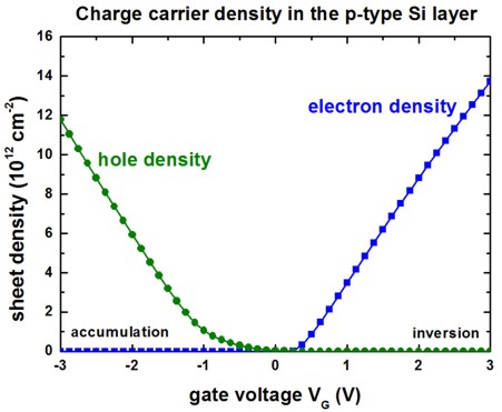
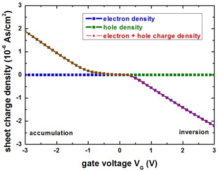
The following figure shows the charge carrier density as a function of bias
voltage.
One can clearly see that in the accumulation regime the hole density dominates
whereas in the inversion regime the electron density dominates the device
behavior.
The electron density can be found in this file: densities/int_el_dens1D.dat
The hole density can be found in this file:
densities/int_hl_dens1D.dat
The relevant column is labeled 'Cl_003', i.e.
cluster-number = 3 and
contains the integrated electron (or hole) density of the region no. 3 which
corresponds to the Si material from 0 nm to 50 nm.
This is the area where we solve the Schrödinger equation.
The following figure shows basically the same data but this time the charge
carrier density has been multiplied
with the elementary charge (e = - 1.6022 * 10-19 As). The red curve is the sum
of electron and hole charge.
Capacitance-voltage curve
-> MIS_CV_3nmSiO2_1D_nn3.in / *_nnp.in

   MIS_CV_1nmSiO2_1D_nn3.in / *_nnp.in
The following figure shows the capacitance-voltage (C-V) curve for the 3
nm thick SiO2 layer (left) and for the 1 nm thick SiO2
layer (right).
The C-V curve has been calculated with the Origin software. Basically we took
the derivative of the total sheet charge density
in the Si substrate (cluster-number = 3)
with respect to the bias voltage.
C = d Q / d V
C is the differential capacitance per unit area.
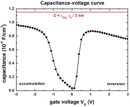 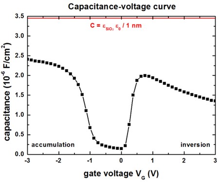
The red line is the calculated capacitance using the
simple approximation of a parallel-plate condensator
which cannot account for the complicated behavior of the real C-V curve.
(Note that the capacitance is a series capacitance, i.e. 1/C is the sum
of 1/Coxide and 1/Csemiconductor.)
In the strong accumulation regime, and in the strong inversion regime, the
space charge layers are very thin and thus the capacity is "approximately equal"
to the insulator capacitance, i.e. it is dominated by the thickness of the
insulating layer (SiO2).
The following parameters were used:
Left figure
SiO2 thickness: 3 nm |
Right figure
SiO2 thickness: 1 nm |
doping concentration: p-type: Nd
= 3 x 1017 cm-3
n-type: Npoly = 5 x 1019 cm-3 |
doping concentration: p-type: Nd
= 1 x 1018 cm-3
n-type: Npoly = 1 x 1020 cm-3 |
Our results are in reasonable agreement with the paper of Richter et al.
In his paper, Richter did not take into account wave function penetration into
the SiO2 barrier.
Consequently and in order to be able to reproduce his results, we also did not
include this effect.
However, wave function penetration can be included easily by extending the
quantum cluster into the SiO2 region.
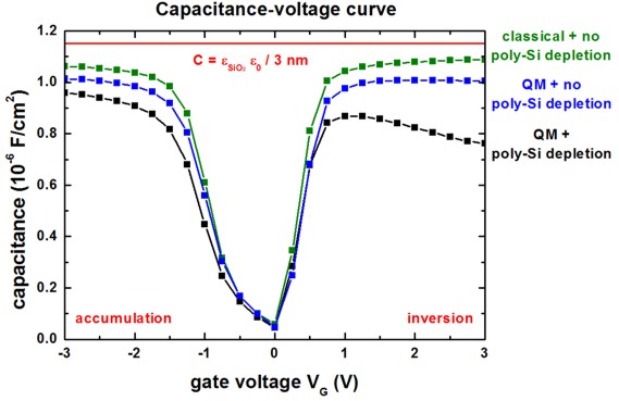
The following figure shows the C-V curve again for the 3 nm SiO2
layer.
Here, we compare the three cases:
- classical
calculation in the p-Si channel, metal contact instead of n-type poly-Si
layer, i.e. the "metal contact region" is excluded from the Poisson equation
- quantum mechanical calculation in the p-Si
channel, metal contact instead of n-type poly-Si layer, i.e. the "metal contact region" is excluded from the Poisson equation
- quantum mechanical calculation in the p-Si channel,
including n-type poly-Si layer depletion
In order to mimick the zero bias condition where we do not have flat bands
(see figure above), we include a workfunction for the metal.
The workfunction of the metal is modeled by a Schottky barrier height of 3.2 V,
so that the minimum of the capacitance alignes with VG = 0 V.
Note: If we simulate a "metal contact", the region from z = -20 nm
to z = -%OxideThickness is exempted from the simulation.
Only the boundary condition (boundary-condition-type =
Schottky) is included at z =
-%OxideThickness.
For the case where we take poly-Si depletion into account (boundary-condition-type
= Fermi), the region from z = -20
nm to z = -%OxideThickness is included in the simulation.
All three cases are in good agreement with Fig. 1 of Richter et al.
One can also plot the surface potential vs. applied gate voltage, e.g. as in Fig. 10
(b) of Chapter 4 of S. M. Sze, Physics of Semiconductor Devices (2007).
 $output-bandstructure

  ...

  potential
= yes !
output electrostatic potential
 output-grid-position                    = 0.0 !
[nm] 0.0
nm, e.g. electrostatic potential vs. voltage
Some comments on the calculations...
- The temperature was set to 300 Kelvin.
- Self-consistent solution of the 1D-Schrödinger-Poisson equation within
the single-band effective-mass approximation (using ellipsoidal effective
mass tensors) for the (Delta) conduction band edges and isotropic masses for
the heavy, light and split-off holes.
The size of the quantum cluster extends from 0 nm to 50 nm.
- The poly-Si depletion has been taken into account (although only
classically and not quantum mechanically).
|