|
| |
nextnano3 - Tutorial
next generation 3D nano device simulator
1D Tutorial
k.p dispersion in bulk GaAs (strained / unstrained)
Author:
Stefan Birner
If you want to obtain the input files that are used within this tutorial, please
check if you can find them in the installation directory.
If you cannot find them, please submit a
Support Ticket.
-> bulk_kp_dispersion_GaAs_nn3.in
/ *_nnp.in          -
input file for nextnano3
/ nextnano++ software
-> bulk_kp_dispersion_GaAs_nn3_3D.in
-
-> bulk_kp_dispersion_GaAs_nn3_strained.in / *_nnp_strained.in -
Band structure of bulk GaAs
- We want to calculate the dispersion E(k) from |k|=0 nm-1 to |k|=1.0
nm-1 along the
following directions in k space:
- [000] to [001]
- [000] to [011]
We compare 6-band and
8-band k.p theory results.
- We calculate E(k) for bulk GaAs at a temperature of 300 K.
Bulk dispersion along [001] and along [011]
  $output-kp-data

 destination-directory    = kp/


 bulk-kp-dispersion       = yes

   grid-position            = 5d0                      !
in units of [nm]
 !----------------------------------------

 ! Dispersion along [011] direction

 ! Dispersion along [001] direction

 ! maximum |k| vector = 1.0 [1/nm]

 !----------------------------------------

 k-direction-from-k-point =
0d0 0.7071d0 0.7071d0 ! [1/nm]
k-direction-to-k-point =
0d0 0d0 1.0d0 !
k-direction
and range for dispersion plot [1/nm]
!
The dispersion is calculated from the k point 'k-direction-from-k-point'
to Gamma, and then from the Gamma point to 'k-direction-to-k-point'.
number-of-k-points = 100 !
 shift-holes-to-zero      = yes
   ! 'yes'
or 'no'
$end_output-kp-data- We calculate the pure bulk dispersion at
grid-position=5d0,
i.e. for the material located at the grid point at 5 nm. In our case this is
GaAs but it could be any strained alloy. In the latter case, the k.p
Bir-Pikus strain Hamiltonian will be diagonalized.
The grid point at grid-position must be located inside a quantum cluster.
shift-holes-to-zero = yes forces the
top of the valence band to be located at 0 eV.
How often the bulk k.p Hamiltonian should be solved can be specified
via number-of-k-points. To increase the resolution, just increase
this number.
- We use two direction is k space, i.e. from [000] to [001] and from [000] to [011].
In the latter case the maximum value
of |k| is SQRT(0.7071² + 0.7071²) = 1.0.
Note that for values of |k| larger than 1.0 nm-1,
k.p theory might not
be a good
approximation any more.Start the calculation.
The results can be found in kp_bulk/bulk_8x8kp_dispersion_as_in_inputfile_kxkykz_000_kxkykz.dat.
Step 3: Plotting E(k)
- Here we visualize the results. The final figure will look like this:
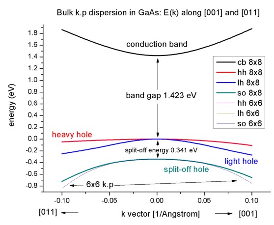
The split-off energy of 0.341 eV is identical to the split-off energy as
defined in the database:
  6x6-kp-parameters = ...
	0.341d0 !  [eV]
- If one zooms into the holes and compares 6-band vs. 8-band k.p, one can
see that 6-band and 8-band coincide for |k| < 1.0 nm
-1 for the heavy and light hole but
differ for the split-off hole at larger |k| values.
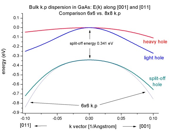
To switch between 6-band and 8-band k.p one only has to change this entry in
the input file:
  $quantum-model-holes

 ...

 model-name = 8x8kp !
for 8-band k.p
            =
  6x6kp !
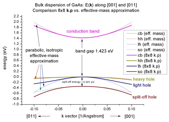
8-band k.p vs. effective-mass approximation
- Now we want to compare the 8-band k.p dispersion with the
effective-mass approximation. The effective mass approximation is a simple
parabolic dispersion which is isotropic (i.e. no dependence on the k
vector direction). For low values of k (|k| < 0.4 nm
-1) it is in good agreement
with k.p theory.
The output data can be find here:
kp_bulk/bulk_sg_dispersion.dat.
Band structure of strained GaAs
- Now we perform these calculations again for GaAs that is strained
with respect to In0.2Ga0.8As. The InGaAs lattice
constant is larger than the GaAs one, thus GaAs is strained tensilely.
- The changes that we have to make in the input file are the following:
  $simulation-flow-control

 ...

 strain-calculation  = homogeneous-strain


  $end_simulation-flow-control
  $domain-coordinates

 ...

 pseudomorphic-on    = In(x)Ga(1-x)As

 alloy-concentration = 0.20d0


  $end_domain-coordinates
As substrate material we take In0.2Ga0.8As and
assume that GaAs is strained pseudomorphically (homogeneous-strain)
with respect to this substrate, i.e. GaAs is subject to a biaxial strain.
- Due to the positive hydrostatic strain (i.e. increase in volume or
negative hydrostatic pressure) we obtain a reduced band gap with respect to
the unstrained GaAs.
Furthermore, the degeneracy of the heavy and light hole at k=0 is
lifted.
Now, the anisotropy of the holes along the different directions [001] and
[011] is very pronounced. There is even a band anti-crossing along [001].
(Actually, the anti-crossing looks like a "crossing" of the bands but if one
zooms into it (not shown in this tutorial), one can easily see it.)
Note: If biaxial strain is present, the directions along x, y or z are not
equivalent any more. This means that the dispersion is also different in
these directions ([100], [010], [001]).
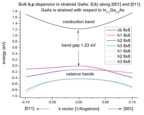
- If one zooms into the holes and compares 6-band vs. 8-band k.p, one can
see that the agreement between heavy and light holes is not as good as in the
unstrained case where 6-band and 8-band k.p lead to almost identical
dispersions.
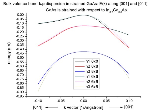
Note that in the strained case, the effective-mass approximation is very poor.
Analysis of eigenvectors
(preliminary)
Using schroedinger-kp-basis = Voon-Willatzen--Bastard--Foreman
(box-integration) one obtains the following output for the eigenvectors
at the Gamma point, k = (kx,ky,kz)
= 0.
The square of the spinor is contained in this file: bulk_8x8kp_dispersion_eigenvectors_squared_000.dat
Example: The X_up component contains a complex number. Here,
we output the square of X_up. This file then gives us information
on the strength of the coupling of the mixed states.
This file is easier to analyze then the file containing the complex numbers (bulk_8x8kp_dispersion_eigenvectors_000.dat).
 eigenvalue  S+     S-
HH
LH     LH     LH     SO
SO

 1           0
1.0    0      0
0      0      0
0

 2           1.0
0      0      0
0      0      0
0

 3           0
0      0      1.0
0      0      0
0

 4           0
0      0      0
1.0    0      0
0

 5           0
0      0      0
0      1.0    0
0

 6           0
0      1.0    0
0      0      0
0

 7           0
0      0      0
0      0      0
1.0

 8           0
0      0      0
0      0      1.0
0
 eigenvalue  S+
S-          X+
Y+          Z+
X-          Y-
Z-

 1
1.0
        0           0
0           0
0           0
0

 2
0
1.0
0           0
0           0
0           0

 3           0
0           0
0           0.5
0.5         0
0

 4           0
0           0
0           0.166
0.166       0.666
0

 5           0
0           0.5
0           0
0           0
0.5

 6           0
0           0.166            0.666
0           0
0                0.166

 7
0           0
0           0
  0.333       0.333
0.333       0

 8
0           0
0.333       0.333
    0
0           0
 0.333
+: spin up, -: spin down
The electron eigenstates are 2-fold degenerate,
i.e. have the same energy, and are decoupled from the holes.
The hole eigenstates are 4-fold (heavy and light holes) and 2-fold degenerate
(split-off holes).
3: |3/2, 3/2>   hh  spin up       1/SQRT(2) | ( X + iY ) up     >


	4: |3/2, 1/2>   lh               1/SQRT(6) | ( X + iY ) down >   -   SQRT(2/3) | Z up   >

	5: |3/2,-1/2>   lh             -1/SQRT(6) | ( X - iY ) up   >  -  SQRT(2/3) | Z down >

	6: |3/2,-3/2>   hh  spin down     1/SQRT(2) | ( X - iY ) down >

	7: |1/2, 1/2>   s/o split        1/SQRT(3) | ( X + iY ) down >   +   1/SQRT(3) | Z up   >

	8: |1/2,-1/2>   s/o split      -1/SQRT(3) | ( X - iY ) up   >  +   1/SQRT(3) | Z down >
up: spin up, down: spin down
	1/SQRT(2) = 0.707  ==>
	1/SQRT(2)^2 = 0.5

	1/SQRT(3) = 0.577  ==>
	1/SQRT(3)^2 = 0.333

	1/SQRT(6) = 0.408  ==>
	1/SQRT(6)^2 = 0.166
|