|
| |
nextnano3 - Tutorial
next generation 3D nano device simulator
1D Tutorial
InAs / In0.4Ga0.6Sb superlattice dispersion with 8-band
k.p (type-II band alignment)
Author:
Stefan Birner,
Michael Povolotskyi
If you want to obtain the input files that are used within this tutorial, please
check if you can find them in the installation directory.
If you cannot find them, please submit a
Support Ticket.
-> 1DInAs_InGaSb_k_zero_nn3.in
/ *_nnp.in -
input file for the nextnano3 and nextnano++ software
-> 1DInAs_InGaSb_k_parallel_nn3.in
- 1DInAs_InGaSb_k_parallel_k_superlattice_nnp.in)
-> 1DInAs_InGaSb_k_superlattice_nn3.in
- 1DInAs_InGaSb_k_parallel_k_superlattice_nnp.in)
-> 1DInAs_InGaSb_SL_k_parallel_k_superlattice_nn3.in / *_nnp.in -
InAs / In0.4Ga0.6Sb superlattice dispersion with 8-band k.p (type-II band
alignment)
This tutorial aims to reproduce Fig. 2(a) of
Long wavelength InAs/InGaSb infrared detectors: Optimization of carrier
lifetimes
C.H. Grein, P.M. Young, M.E. Flatte, H. Ehrenreich
J. Appl. Phys. 78 (12), 7143 (1995)
Conduction and valence band edges
-> 1DInAs_InGaSb_k_zero_nn3.in
The heterostructure is a superlattice with 3.98 nm InAs and 1.5
nm In0.4Ga0.6Sb, where both constituents are
strained with respect to the GaSb substrate.
The structure has a type-II band alignment, i.e. the electrons are
confined in the InAs layer,
whereas the holes are confined in the In0.4Ga0.6Sb layer.
The In0.4Ga0.6Sb layer is strained pseudomorphically with
respect to the GaSb substrate,
leading to a compressive strain (-2.5 %) which splits the
degeneracy of the heavy and light hole band edges in this layer.
Thus, the heavy hole band edge lies above the light hole band edge.
The InAs layer is also strained pseudomorphically with respect to the GaSb
substrate,
and is thus under slight biaxial tension (+0.6 %).
The splitting of the hole band edges is the opposite as in InGaSb, i.e. the
light hole band edge is above the heavy hole band edge.
The following figure shows the electron and hole band edges.
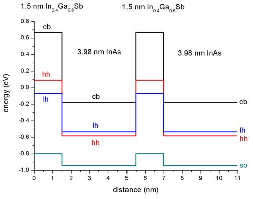
The origin of the energy scale is set to the GaSb valence band edge energy.
Electron and hole wave function for k|| = 0
- We simulate one period only (i.e. from 0 nm to 5.48 nm) and solve
the Schrödinger equation with periodic boundary conditions to mimic an
infinite superlattice.
The following figure shows the conduction band edge and the heavy, light and
split-off hole valence band edges in this superlattice structure
together with the electron (c1), heavy hole (hh1)
and light hole (lh1) energies and
wave functions (psi²), calculated within 8-band k.p theory.
One can clearly see that the electron state (c1) is confined in the
InAs layer (right part of the figure),
whereas the heavy (hh1) and light hole (lh1)
states are confined in the In0.4Ga0.6Sb layer (left part
of the figure).
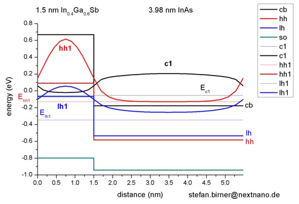
We used the same material parameters as given in the above cited paper by
Grein et al., apart from the k.p parameters.
Electron and hole energies for k|| /= 0
-
-> 1DInAs_InGaSb_k_parallel_nn3.in
The following figure shows the E(k||) dispersion of the
electron ground state and the two highest hole states along two different
directions in (kx,ky) space.
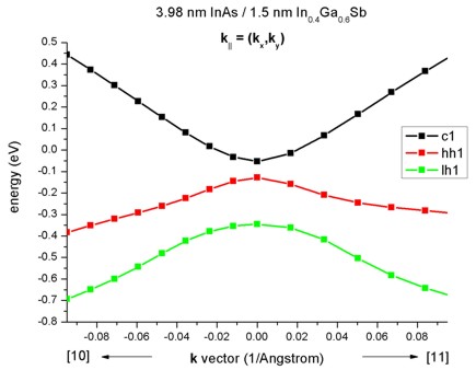
This data is contained in this file:
Schroedinger_kp/par1D_disp_01_00_11_hl_8x8kp_ev_min001_ev_max010.dat
Note that the band gap is not determined by the bandgap of one individual
layer. It is determined by the electron ground state in the InAs layer, and
the hole ground state in the InGaSb layer. This means more freedom for band
gap engineering.
Electron and hole energies for kz /= 0
-
-> 1DInAs_InGaSb_k_superlattice_nn3.in
The right part of the following figure shows the E(kz) superlattice
dispersion of the electron ground state and the two highest hole states. kz
is the superlattice vector between 0 and 1 pi/L where L = 5.48 nm is the length of one
superlattice period.
(1 pi/L = 0.0573 1/Angstrom)
This data is contained in this file:
Schroedinger_kp/8x8kp_dispSL_hl_qc001_evmin001_evmax016.dat
The left part of the figure shows the E(k||) dispersion
along [10], i.e. from (kx,ky) = (0,0) to (kx,ky)
= (-0.1,0) which is shown in the figure above already.
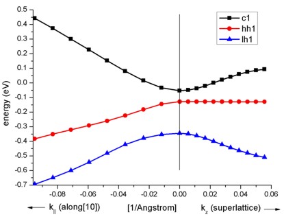
One can clearly see that these heterostructure bands are highly nonparabolic.
- The resolution of the kz superlattice vectors is specified
here:
 $quantum-model-electrons

  ...

  num-ks-001  = 11
  !
number of superlattice vectors in [001] direction
  ...


 $quantum-model-holes

  ...

  num-ks-001  = 11
  !
- The number of superlattice vectors to be put out is specified here:
 $output-kp-data

  ...

  cb-k-SL-min = 1
  !
  cb-k-SL-max = 11
! num-ks-001)
  ...

  vb-k-SL-min = 1
  !
  vb-k-SL-max = 11
! num-ks-001)
-
-> 1DInAs_InGaSb_SL_k_parallel_superlattice.in
This input file generates a 3D plot of the the energy dispersion E(kx,ky,kSL)
for each eigenvalue. The files are called
dispersion_k_parallel_k_SL_ev001.fld
where ev001 indicates eigenvalue number 1.
|