www.nextnano.com/documentation/tools/nextnano3/tutorials/1D_TightBinding_bulk.html
nextnano3 - Tutorial
next generation 3D nano device simulator
Empirical tight-binding (sp3s*) band structure of GaAs, GaP,
AlAs, InAs, C (diamond) and Si
  -> 1D_TightBinding_bulk_GaAs.in

  -> 1D_TightBinding_bulk_GaAs_so.in

  -> 1D_TightBinding_bulk_Al0.3Ga0.7As.in

  -> 1D_TightBinding_bulk_GaP.in

  -> 1D_TightBinding_bulk_GaP_so.in

  -> 1D_TightBinding_bulk_AlAs.in

  -> 1D_TightBinding_bulk_AlAs_so.in

  -> 1D_TightBinding_bulk_C.in

  -> 1D_TightBinding_bulk_Si.in

  -> 1D_TightBinding_bulk_Ge.in

  -> 1D_TightBinding_bulk_InAs_so.in

  -> 1D_TightBinding_bulk_AlSb_so.in

  -> 1D_TightBinding_bulk_InSb_so.in

  -> 1D_TightBinding_bulk_Al0.5In0.5Sb.in
Empirical tight-binding (sp3s*) band structure of GaAs and GaP
The empirical tight-binding model that is used here is based on the sp3s*
Hamiltonian, i.e. the 10 x 10 matrix given in Table (A) of
[Vogl]
A semi-empirical tight-binding theory of the electronic structure of
semiconductors
P. Vogl, H.P. Hjalmarson, J.D. Dow
J. Phys. Chem. Solids 44 (5), 365 (1983)
Download the paper including corrections.
In addition, we include spin-orbit coupling leading to a 20 x 20 matrix.
The additional terms arising due to spin-orbit coupling are given for instance
on p. R5 of
Microscopic theory of nanostructured semiconductor devices: beyond the
envelope-function approximation
A. Di Carlo
Semiconductor Science and Technology 18, R1 (2003)
We note that nowadays much better theoretical methods are available for calculating the
band structure of bulk materials.
However, for educational purposes, the chosen sp3s* method should be
sufficient.
In this tutorial, we calculate the bulk band structure of
- GaAs, GaP and AlAs without spin-orbit coupling using
the parameters of
[Vogl] at T =
0 K
- GaAs, GaP and AlAs including spin-orbit coupling using the parameters
of
[Klimeck] at T = 300 K
[Klimeck]
sp3s* Tight-Binding parameters for transport simulations in compound
semiconductors
G. Klimeck, R.C. Bowen, T.B. Boykin, T.A. Cwik
Superlattices and Microstructures 27 (5), 519 (2000)
Input
The values for the tight-binding parametrization have to be specified in the
input file:
	$numeric-control

 ...

 !------------------------------------------------------------------------------

 ! Tight-binding parameters for GaAs (values of [Klimeck]). The units are
	[eV].

 !------------------------------------------------------------------------------

 !tight-binding-parameters = -3.53284
	! Esa (GaAs)


	0.27772
	! Epa


	-8.11499
	! Esc


	4.57341
	! Epc


	12.33930
	! Es_a


	4.31241
	! Es_c


	-6.87653
	! Vss


	1.33572
	! Vxx


	5.07596
	! Vxy


	0.0
	! Vs_s_


	2.85929
	! Vsa_pc


	11.09774
	! Vsc_pa


	6.31619
	! Vs_a_pc


	5.02335
	! Vs_c_pa


	0.32703  0.12000  ! Delta_so_a
	Delta_so_c

 ! Note: a = anion, c = cation

 !       s_ = s*
For more information about the meaning of these parameters, we refer to the
above cited references.
Output
The output of the calculated tight-binding band structure can be found in the
following file:
TightBinding/BandStructure.dat
The first column contains the number of the grid point in the Brillouin zone.
These grid points run
- from L point to Gamma point (along Lambda)
- from Gamma point to X point (along Delta)
- from X point to the U,K points
- from U,K points to Gamma point (along Sigma).
The next columns are the eigenvalues of the tight-binding Hamiltonian in units
of [eV] for each grid point in k = (kx,ky,kz)
space.
The file
TightBinding/BandStructure_without_so.dat
contains the tight-binding band structure without spin-orbit coupling.
The file
TightBinding/k_vectors.dat
contains for each point the information to which k point it belongs to.
 no.  kx
ky           kz
   |k|
kx[2pi/a]    ky[2pi/a]    kz[2pi/a]
|k|[2pi/a]

 1    0.314159E+01 0.314159E+01
0.314159E+01 0.544140E+01 0.500000E+00 0.500000E+00 0.500000E+00
0.866025E+00

 ...
Note: Currently the units of kx, ky and kz
do not take into account the lattice constant a. This should be modfied.
The values for kx, ky and kz in units of
[2pi/a] are correct, however.
Another improvement would be to calculate and output the three-dimensional
energy dispersion E(kx,ky,kz),
and two-dimensional slices E(kx,ky,0) through the
three-dimensional energy dispersion E(kx,ky,kz)
for a constant value of kz, e.g. kz = 0.
Results
GaAs without spin-orbit coupling
-> 1D_TightBinding_bulk_GaAs.in
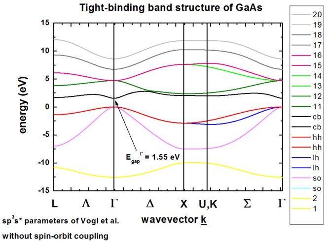
The calculated band structure is in excellent agreement with Fig. 11(d) of
[Vogl].
The conduction band minimum is at the Gamma point (direct band gap).
Because spin-orbit coupling is not included in the Hamiltonian,
heavy, light and split-off hole are degenerate at the Gamma point, i.e. at k
= (kx,ky,kz) = 0.
The sp3s* empirical tight-binding parameters were taken from
[Vogl] at T = 0 K.
GaAs including spin-orbit coupling
-> 1D_TightBinding_bulk_GaAs_so.in
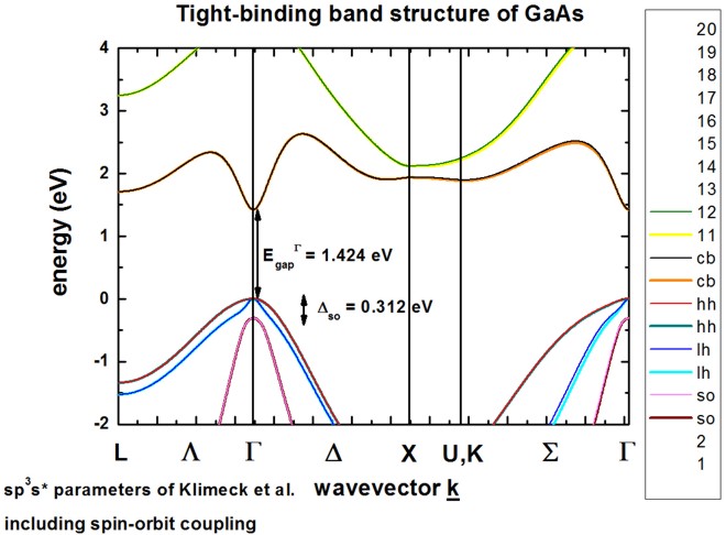
The calculated band structure is in excellent agreement with Fig. 1 of
[Klimeck].
The conduction band minimum is at the Gamma point (direct band gap).
Spin-orbit coupling lifts the degeneracy of heavy/light hole and split-off hole
at the Gamma point.
Heavy and light hole are still degenerate at the Gamma point.
The sp3s* empirical tight-binding parameters were taken from
[Klimeck] at T = 300 K.
GaP without spin-orbit coupling
-> 1D_TightBinding_bulk_GaP.in
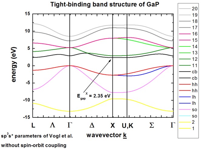
The calculated band structure is in excellent agreement with Fig. 2 of
[Vogl].
The conduction band minimum is calculated to be at the X point (indirect band
gap).
Because spin-orbit coupling is not included in the Hamiltonian,
heavy, light and split-off hole are degenerate at the Gamma point, i.e. at k
= (kx,ky,kz) = 0.
The sp3s* empirical tight-binding parameters were taken from
[Vogl] at T = 0 K.
GaP including spin-orbit coupling
-> 1D_TightBinding_bulk_GaP_so.in
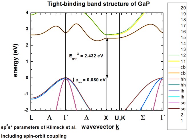
The calculated band structure is in excellent agreement with Fig. 1 of
[Klimeck].
The conduction band minimum is in the vicinity of the X point at the Delta line
(indirect band gap), so-called camel's back.
Spin-orbit coupling lifts the degeneracy of heavy/light hole and split-off hole
at the Gamma point.
Heavy and light hole are still degenerate at the Gamma point.
The sp3s* empirical tight-binding parameters were taken from
[Klimeck] at T = 300 K.
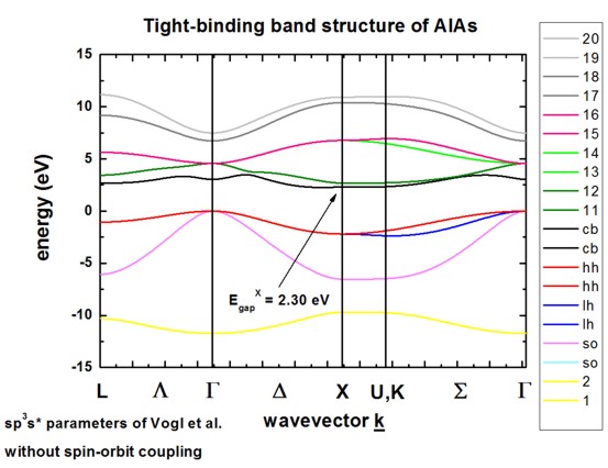
AlAs without spin-orbit coupling
-> 1D_TightBinding_bulk_AlAs.in
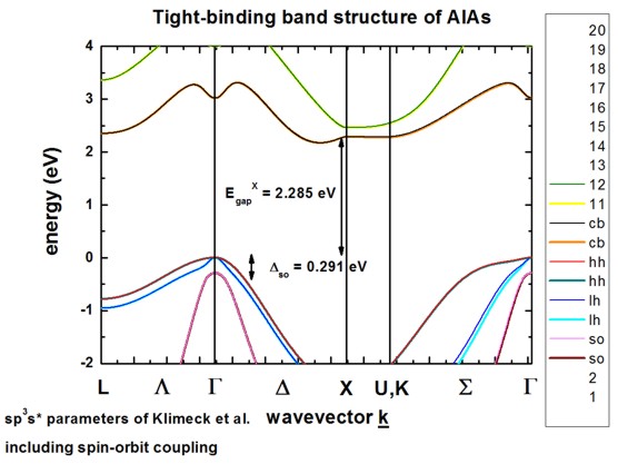
AlAs including spin-orbit coupling
-> 1D_TightBinding_bulk_AlAs_so.in
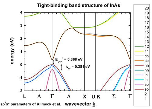
InAs including spin-orbit coupling
-> 1D_TightBinding_bulk_InAs_so.in
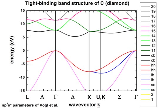
C (diamond) without spin-orbit coupling
-> 1D_TightBinding_bulk_C.in
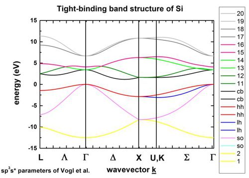
Si (silicon) without spin-orbit coupling
-> 1D_TightBinding_bulk_Si.in
The k space resolution, i.e. the number of grid points on the axis of these
plots can be adjusted.
  $tighten

   calculate-tight-binding-tighten = no
!

   destination-directory
= TightBinding/

   number-of-k-points
= 50
!
This corresponds to 50 k
points between the Gamma point and the X point.
!
|