|
| |
nextnano3 - Tutorial
next generation 3D nano device simulator
2D Tutorial
Ultrathin-body Double Gate FET - DG MOSFET (Double Gate Metal Oxide Semiconductor Field Effect
Transistor)
Author:
Stefan Birner
-> 2DDoubleGateMOSFET_nn3_05grid.in / *nnp*.in - input file for the nextnano3 and nextnano++ software
(2D simulation)
-> 3DDoubleGateMOSFET_nn3_05grid.in
-
input file for the nextnano3 software
(3D simulation)
These input files are included in the latest version.
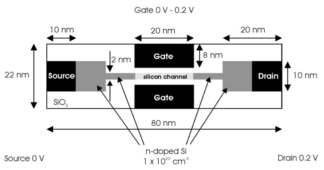
DG MOSFET (Double Gate Metal Oxide Semiconductor Field Effect
Transistor)
The main idea of a Double Gate MOSFET is to control the Si channel very
efficiently by choosing the Si channel width to be very small and by
applying a gate contact to both sides of the channel. This concept helps to
suppress short channel effects and leads to higher currents as compared with
a MOSFET having only one gate.
- Double Gate MOSFET (Metal Oxide Semiconductor Field Effect
Transistor)
(grown
on Si substrate, i.e. unstrained)
The Double Gate MOSFET contains the following regions
|
cluster |
region |
|
color |
|
| 1 |
1 |
Source and drain
are connected with the Si channel |
blue |
|
| 2 |
2 |
Source (metal) |
left |
|
| 3 |
3 |
Drain (metal) |
right |
|
| 4 |
4 5 |
Gate / Backgate (metal) |
top/bottom |
|
| 5 |
6 7 |
Doped source and drain
region (Si) |
blue |
|
| 6 |
8 |
The insulating material is SiO2. |
red |
(default
region) |
Both the regions 4 (gate) and 5 (backgate) form the cluster no. 4.
The width of the Si channel is 2 nm.
The distance between the two gates is 6 nm, i.e. the isolating SiO2
is 2 nm thick on each side. The width of the two gates is 20 nm.
The distance between source and drain is 60 nm. The widths and the lengths of
source, drain, left and right doped source regions are 10 nm x 10 nm each. The
length of the 2 nm Si channel (without the square doped source and drain regions) is 40
nm.
| |
Top gate (Schottky barrier 3.445 V)
0 V ... 0.2 V |
|
|
Source (0.0 V) |
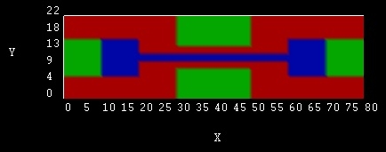 |
Drain (0.2 V) |
| |
Bottom gate (Schottky barrier 3.445 V)
0 V ... 0.2 V
Schematic top view of the Double Gate
MOSFET |
|
The blue squares (Si) are n-doped with a a
concentration of 1x1020 cm-3.
The 2 nm channel
is n-doped with the same concentration from 20 to 30 and from 50 to 60 nm.
 $doping-function


  doping-function-number = 1
  !
Source
  impurity-number        =
  1

  doping-concentration   = 1d2
  ! 1 x 1020 cm-3

  only-region
  = 0d0 20d0
  6d0 16d0  !
  xmin xmax ymin ymax


  doping-function-number = 2
  !
  impurity-number        =
  1

  doping-concentration   = 1d2
  ! 1 x 1020 cm-3

  only-region
  = 20d0 30d0
  10d0 12d0 ! xmin
  xmax ymin ymax


  doping-function-number = 3
  !
  impurity-number        =
  1

  doping-concentration   = 1d2
  ! 1 x 1020 cm-3

  only-region
  = 50d0 60d0
  10d0 12d0 ! xmin
  xmax ymin ymax


  doping-function-number = 4
  !
  impurity-number        =
  1

  doping-concentration   = 1d2
  ! 1 x 1020 cm-3

  only-region
  = 60d0 80d0
  6d0 16d0  !
  xmin xmax ymin ymax


 $end_doping-function


 $impurity-parameters

  impurity-number
  = 1

  impurity-type
  = n-type

  number-of-energy-levels     = 1

    energy-levels-relative      =
0.044d0 ! [eV]
degeneracy-of-energy-levels = 2
! degeneracy of energy levels, 2 for n-type
$end_impurity-parameters
- At the two gates we apply a Schottky barrier of 3.443 eV:
 $poisson-boundary-conditions
  ...
  poisson-cluster-number  =
  3
  !
top and bottom gate
  region-cluster-number   =
  4
  applied-voltage         =
  0d0
  boundary-condition-type =
  schottky
  schottky-barrier        =
  3.443d0
  contact-control         =
  voltage
  ...
$end_poisson-boundary-conditions
The source and drain contacts are ohmic.
- Source: 0.0 V
- Drain: 0.2 V
A voltage sweep varies the gate (top gate and bottom gate) voltage from 0 to
2.0 V in 10 steps.
 $voltage-sweep

  sweep-number
  = 1

    sweep-active
  = yes

  poisson-cluster-number  = 3
  !
Gate: poisson-cluster-number = 3
step-size
= 0.1d0
number-of-steps =
10
data-out-every-nth-step = 1
$end_voltage-sweep
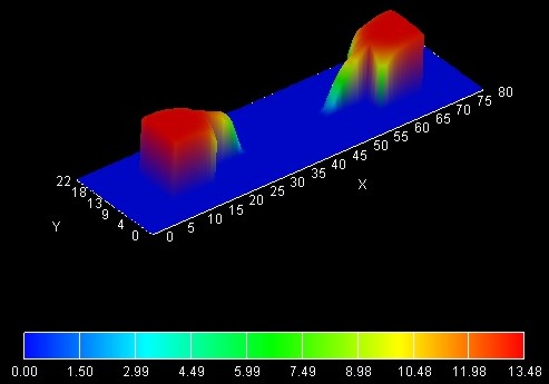
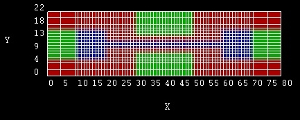
- Gridding
|
 |
|
Grid lines of the Double Gate
MOSFET
Note: The grid lines that are shown in the figure are the
material grid lines. The grid lines that one specifies in the input file
are the physical grid lines. The material grid lines are placed
half-way between the physical grid lines. For more information on the
definition of the grid confer this page:
Grids and Geometry |
How to run the input file...
- The lattice temperature is taken to be 300 Kelvin.
The
flow scheme is 4 for a
classical self-consistent calculation:
- calculate nonlinear Poisson classically
- calculate current classically
No strain will be considered here.
- This time we perform a two-dimensional simulation. The overall
simulation domain, that is the real space region in which the device is
defined, is taken to be a rectangle having the size 22 nm x 80 nm.
- Just a reminder: If you need additional information about the keywords and
their specifiers, you can look them up
here.
- Output
- The band structure (conduction and valence bands) will be saved into the directory band_structure/.
densities/.
current/.
raw_data/.
Output files that will be produced are:
Results
- The current-voltage (I-V) characteristic can be found in the following
file:
current/IV_characteristics2D.dat
The drain voltage is kept constant at 0.2 V, the gate voltage varies from
0 to 2.0 V.
The figure shows the I-V characteristics for three different mobility
models, compared with the results obtained with a commercial software
package. The units for the current in a 2D simulation are [A/m] (but can
be adjusted to [A/cm]).
- mobility-model-simba-0
(no dependence on electric field)
-
mobility-model-simba-2 (mobility depends on parallel electric field)
In this case the current is smaller because the mobility
decreases when the applied voltage increases.
-
mobility-model-lom (Lombardi mobility
model)
- $mobility-model-simba
- $mobility-model-lom
(Lombardi mobility model)
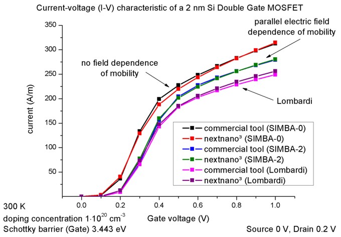
Note: This is a classical calculation. So no quantum
mechanical effects are included.
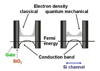
For a quantum mechanical calculation, the current is smaller. This is
mainly due to the difference in the classical and quantum
mechanical electron density.
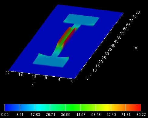
|
 |
|
Classical and quantum mechanical electron density as
seen when cutting through the Si channel.
(Note: In this figure, the Si channel is larger than 2 nm.)
In the classical simulation, the electron density has its maximum at
the SiO2-Si interface.
In the quantum mechanical simulation, however, the electron density is
basically zero at the SiO2-Si interface. |
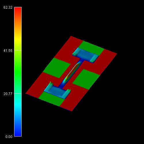
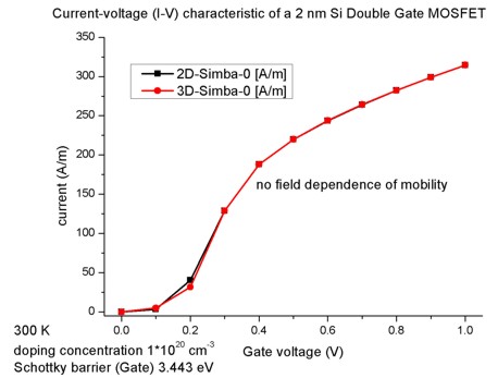
3D
-> 3DDoubleGateMOSFET_nn3_05grid.in
In order to test the nextnano³
implementation of the three-dimensional drift-diffusion current, we calculated
this Double Gate MOSFET in a three-dimensional simulation. We assume that the
structure is homogeneous along the z direction and assume the z direction to be
10 nm long (grid spacing 2 nm). The units of the current are in [A] (current/IV_characteristics3D.dat).
The current has to be divided by the length of the device along the z direction,
i.e. by 10 nm, in order to obtain it in units of [A/m]. The 3D results are in
agreement with the 2D results.
|
 |
|
Comparison of the 2D and 3D nextnano³
results for mobility-model-simba-0. |
|