|
| |
1D Tutorial: Simple SiGe structure
- Here are the input files:
input_file1.in -
simple SiGe structureinput_file2.in -
include currentinput_file3.in -
include quantum models (single-band Schrödinger equation)input_file4.in
- read in raw data and solve 6-band k.p Schrödinger equation
Now it's time to get started...
(This is a tutorial from 2001. It is more than 19 years
old. At that time, nextnano³
was a command line tool. Some parts of the documentation are not really necessary or applicable any more,
or are just optional. For backwards compatibility, they are still there but they
are shown in light gray
color. Some material parameters in the database have changed since then (e.g.
band edges). Therefore, one cannot reproduce all figures exactly as they are
shown here. Also, the semiconductor structures in this tutorial are a bit
artificial. Nevertheless, this tutorial might be helpful to give you a
decent introduction into the nextnano³ software.)
- Step 1: Simple SiGe structure
These input files are needed by the nextnano³
executable:
- ..\database\database_nn3.in -
contains
parameters of the materials (don't worry about it now)
- In this tutorial, you have four options for the input file:
Start with input_file1.in - a simple SiGe structure.
- Open
input_file1.in
with nextnanomat and read it. There are lots of comments that
will explain you what's going on.
If you have any questions regarding the keywords you will find it
extremely useful to right-click on your mouse within the nextnanomat text
editor. Then a link to the online documentation appears, or have a look at the explanations
here.
First we try a simple structure consisting of two regions of SiGe and
different alloy concentrations. Since the structure is grown pseudomorphically on
Si, the bands are split by strain (different lattice constants,
lattice mismatch 4 %).
- No current or quantum states will be calculated.
- It's a 1D simulation.
- Since we only want a classical self-consistent simulation we choose
  flow-scheme =
	4
.
This choice means that we are first calculating the built-in potential with the
classical nonlinear Poisson equation.
Then the program is calculating a self-consistent solution of
the classical Poisson and current equation (if current calculation is specified in the input file -
in our case it is not).
- Output
For the output the destination directories are free to choose, whereas
(most of) the
file names are fixed and incorporate all information of the file.
- The band structure will be saved into the directory band_structure/
- The densities will be saved into densities/
- The strain will be saved into strain/
- Now run the executable by pushing the green button and have a look at the output files
with nextnanomat.
Alternatively, you can of course use any other
graphics packages as well (e.g. Origin, gnuplot, Matlab, MS Excel, ...).
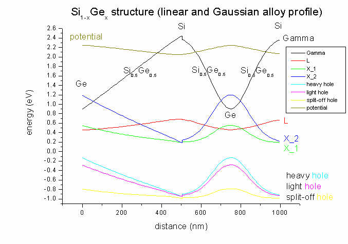
- The structure consists of two alloy concentrations of Si1-xGex.
The left part has a linear profile (starting with
x=1,
i.e. Ge), the right part is gaussian (with x=1, i.e.
Ge at the maximum).
$material

  ...

    material-name        =
  Si(1-x)Ge(x)  !


  $alloy-function

  ...

  function-name        =
  linear
  !

  xalloy-from-to       =
  1d0 0d0
  !
Ge at 0 nm, Si at 500 nm
  vary-from-pos-to-pos = 0d0 500d0     !


  ...

  function-name        =
  gaussian-1d
  !

  gauss-center         =
  750d0
  !

  gauss-width          =
  100d0
  !
  xalloy-minimum       =
  0d0
  !
  xalloy-maximum       =
  1d0
  !
- In the directory
band_structure/
you will find files containing ASCII data (1st column:
position in nm, 2nd column: energy in eV).
The meaning of the abbreviations is the following:
cb1D_Gamma.dat - conduction band 1 (Gamma band)
cb1D_L.dat - conduction band 2 (L
band)
cb1D_X.dat - conduction band 3 (X
band, Here: They are split due to strain) (to be precise: It is Delta
for Si and not X.)
vb1D_hh.dat - valence band 1 (heavy
hole)
vb1D_lh.dat - valence band 2 (light
hole)
vb1D_so.dat - valence band 3 (split-off hole)
BandEdges1D.dat - all conduction and valence band edges
potential.dat - electrostatic potential (from Poisson
equation)
Both Si and Ge are indirect semiconductors. Bulk Si has its conduction band
minimum at the Delta point (500 nm / 1000nm) (we call it X here for
simplicity) whereas Ge has its conduction band
minimum at the L point (0 nm / 750 nm)).
- As the substrate is Si, and the structure is grown pseudomorphically on
Si, there will be strain due to the Si-Ge lattice mismatch of 4 %
whenever a fraction of Ge is present. In the case of pure Si (at 500 nm) there
will be no strain and therefore no splitting of the degenerate X conduction
band. In the case of finite strain, the X band degeneracy is lifted,
leading to a second X conduction band.
Similarly for the heavy and light hole bands: At 500 nm (Si only, no strain)
heavy and light hole are degenerate. This degeneracy is lifted when strain is
applied through the incorporation of Ge.
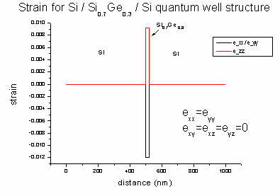
The strain tensor has six dimensionless components (exx, eyy,
ezz, exy, exz, eyz) and its values
are written to strain/strain_cr1D.dat. The ASCII file contains in its
columns: position in nm, exx, eyy, ezz, exy,
exz, eyz).
In our example file all offdiagonal strain components (exy, exz,
eyz) are zero and exx is equal to eyy. The
strain has its maximum value when pure Ge is present (0 and 750 nm).
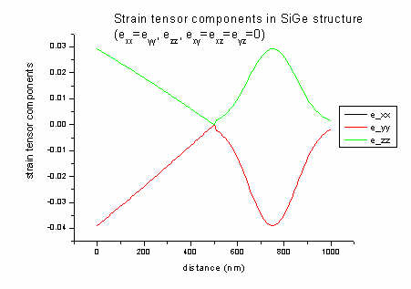
In 1D strain can be calculated analytically:
a = lattice constant [nm] (Si: 0.543; Ge: 0.565)
c11, c12 = elastic constants [GPa] (Si:
165.77, 63.93; Ge: 128.53, 48.26)
biaxial strain: e|| = exx = eyy
= ( asubstrate - alayer ) / alayer = ( 0.543
- 0.565 ) / 0.565 = - 0.039 (4 % lattice mismatch)
strain along growth direction: ezz =
- 2c12 / c11 e||
= - 2 * 48/129 * (- 0.039) = 0.029
These equations are valid for zinc blende in [001] growth direction assuming
pseudomorphic (=commensurate) epitaxial growth. In this case, shear strain is zero.
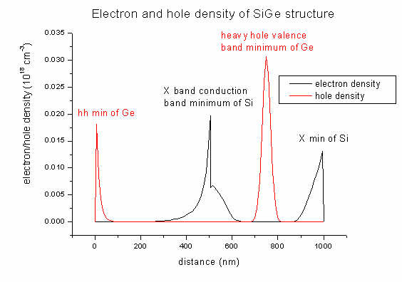
- In the
densities
directory you will find output for the electron and hole densities of our SiGe
structure (and also the space charge):
density1Del.dat - contains electron density
(1st column: distance in nm, 2nd column: density
in 1018
cm-3)
density1Dhl.dat
  -
contains hole density
density1DGamma_L_X.dat - contains electron density
for each band (Gamma, L, X)
density1Dh_lh_so.dat - contains
hole density for each band (heavy hole, light hole, split-off hole)
density1Dpiezo.dat
  -
contains piezoelectric charges
(important for III-V semiconductors in [110] and [N11] growth
directions
==> piezoelectric field, see Piezo Tutorial)
density1Dpyro.dat - contains pyroelectric charges
(important for pyroelectric materials with wurtzite structure like GaN,
AlN and InN
==> spontaneous polarization ==> pyroelectric field)
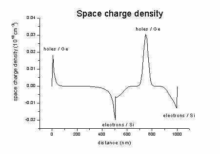
density1Dspace_charge.dat -
contains the space charge density (here: no donors and acceptors
present)
= - electron density + hole density +
ionized donors - ionized acceptors
interface_densitites1D.txt - contains information about the piezo
and pyroelectric charge densities at
interfaces (position in nm of interface and 2D interfacial number
density in units of [1012
cm-2].
The electron/hole density output will be given in units of [1018
cm-3].
These units are the same for 1D, 2D and 3D simulations.
Note: The pictures shown below were created with a
previous version of nextnano³. Meanwhile the parameters in the database have
changed (as well as some bugs were fixed). So the pictures do not necessarily
have to coincide with the results obtained from the current version of
nextnano³. Especially in this example, the density depends very critically on
tiny changes in the database parameters.
The space charge in our case looks like this (sum of hole minus electron
density).
- Step 2: Include current
Now let's move on to input_file2.in.
- Now we try to put some dopants into our structure and apply some voltage
to see if there is a current.
For dopants we need:
- doping functions
- impurity parameters
For the current we need:
- contacts (Poisson boundary conditions)
- current regions and
clusters
- current models
For the contacts we use two additional regions of material Metal, located at
the edges of the simulation region.
First run without applied voltage and after that try with different applied
voltages but not larger than 0.1 V. (For larger voltages you should solve the
equations step wise ==>
voltage sweep.)
In order to see the effects of doping, we take simpler alloy functions, namely
constant alloys, i.e. our structure consists of Si only.
- Doping
First you have to specify a doping profile. This can be done by the keyword
$doping-function.
only-region.
The first profile is a constant doping with concentration 1d1 *
1018/cm3 (1d1 = 1*101 = 10).
The second profile is a well with double Gaussian walls. The walls are centered
at parameter center and the slope of the walls is given by width.
The doping concentration is at the position specified by the specifier
position (optional for constant doping profile).
The function is normalized such that the result is doping concentration at
position position.
The impurity number specifies the kind of impurities used in the profile.
Consider the degeneracy factor of the impurity levels (2 for donors and 4 for
acceptors). For details please confer
$impurity-parameters.
We take a Si structure with constant n-type doping between 100 nm and 200 nm
(1*1019 cm-3) and a p-type doping well (with Gaussian
walls centered at 600 and 800 nm (1*1018 cm-3) ).
- Current
In order to apply any voltage to the device you have to define contacts. This
is done by the
Poisson boundary conditions. There are mainly two different
kinds:
- Schottky (implies a Schottky barrier, can be used to simulate
surface states)
- ohmic (no barrier)
These Poisson clusters are assigned to the region-clusters that should serve
as the contacts. (Here they consist of the material Metal but the material
name can be arbitrary as the contacts are not included in the
Poisson,Schrödinger or current equation.).
The voltage difference should not be too large because of convergence
issues. Larger voltage should be calculated stepwise using
voltage-sweep or
adjusting them manually by reading in the previous potential and Fermi levels.
To calculate the current flow due to the applied voltage in the
Poisson
boundary conditions, one has to specify certain
current regions and
clusters
analogous to the material and
quantum clusters. On each cluster one can apply
a certain current model (so far only simple drift-diffusion but there is more
to come).
It is possible to specify different regions for different current models but
since so far only one model is implemented, you can skip the
current region
keyword. By not specifying any region, the whole simulation area is region
number 1. Then a current cluster containing this region 1 has to be specified.
Mobility parameters for all materials contained in the
current cluster have to
be present either in the database or in the
input file. For now, also for the
metal contacts, mobility parameters have to exist although they are not used
in the calculation.
- Output
- The band structure will be saved into the directory band_structure/
- The densities will be saved into densities/
- The strain will be saved into strain/
- The current will be saved into current/
Note: Please add the specifier IV-curve-out =
yes to the keyword
$output-current-data in order to print out current data (I-V
characteristics). (The file
current.dat will only contain zeros.)
$output-current-data
...
 IV-curve-out =
	yes
- Now run the executable
and have a look at the output files.
- Current is set to
-0.1 V.
applied-voltage = -0.1d0 ! [V]
- The band structure (conduction and valence bands) and the potential looks
like this:
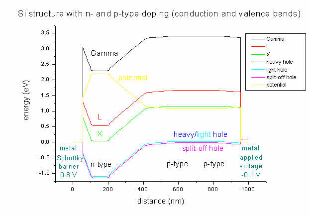
As boundary conditions, on the left side a Schottky barrier of 0.8 V is
assumed whereas on the right side a voltage of -0.1 V is applied.
As can be seen, the lowest conduction band in Si is the
X band. Strain is zero in this case (Si pseudomorph on Si), thus
heavy and light hole
bands are degenerate and there is no X band
splitting (compare input_file1.in).
It can clearly be seen that the area with heavy n-type doping (between 100 and
200 nm) "pulls down" the conduction band. The electrostatic potential (yellow
line) has its highest value in the n-type region and its lowest in the
p-type region (between 600 and 800 nm).
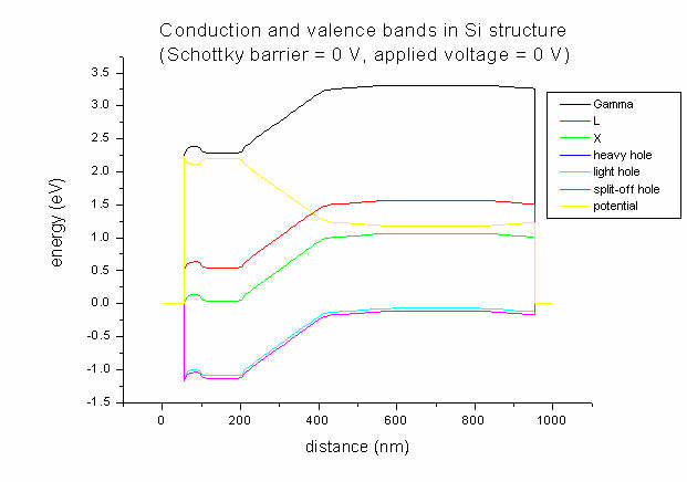
- For comparison only, here's the band structure for the same doping profile
but with Schottky barrier = 0 V and applied voltage = 0 V.
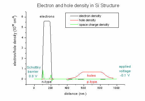
- Now let's go back to our
input_file2.in.
Here we plot the electron and hole densities (and also the space charge
density; units 1018 cm-3):
- The n and p mobilities:
The mobility output mobility1D.dat is on a different grid (as well
as the drift velocities and the current) -> see
material grid vs. physical
grid for details).
Electron (black line) and hole mobilities (red line)
in Si structure (applied voltage: -0.1 V)
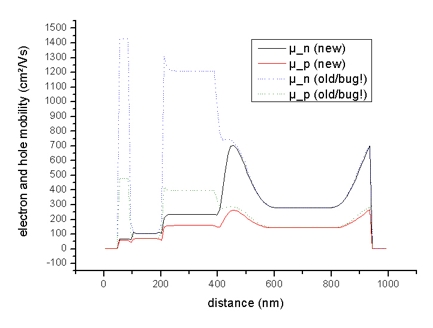
(The dotted lines should be ignored!)
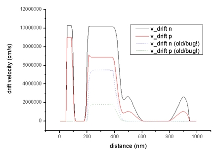
- The diagrams of the drift velocity vd,n (electrons) and vd,p
(holes):
drift_velocity1D.dat - units: cm/s
Drift velocities of electrons (black line) and holes (red
line) in Si structure (applied voltage: -0.1 V)
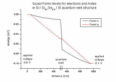
- The quasi-Fermi levels for n (electrons) and p (holes):
FermiLevel1D.dat - quasi-Fermi level for electrons and for holes
The difference between left and right boundaries is the applied voltage of
-0.1 V.
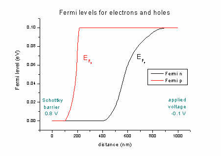
If no voltage is applied the quasi-Fermi levels are constant (no current
flow). Our ansatz for the current: It is proportional to the mobility and to
the gradient of the quasi-Fermi level (drift-diffusion model).
More details for the current output can be found
here.
currentD.dat
The total current that is flowing is jtot = jel
+ jhl = 2.45 * 10-8 A/m2 + 0.24 * 10-8
A/m2 = 2.70 * 10-8 A/m2.
- Now, let's switch current off.
applied-voltage = 0.0d0 ! [V]
The quasi-Fermi levels are constant (zero) (FermiLevel1D.dat).
The drift velocities are zero (drift_velocity1D.dat).
Obviously, the current flow is zero (currentD.dat).
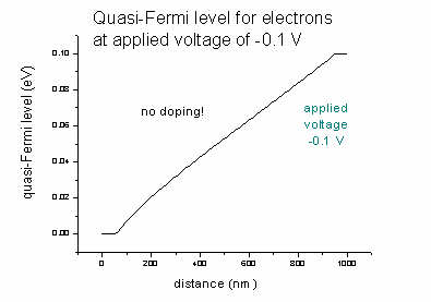
- If we had no doping, the effect of an applied voltage of
-0.1
V for the quasi-Fermi level EF,n of the electrons would be (same
for EF,p):
- Step 3: Include quantum models (1-band Schrödinger equation)
Now let's include quantum models. Have a look at
input_file3.in.
So far we only used classical electrostatics which is fast but not very
interesting.
If you have small structures where quantization effects are no longer
negligible then you might include either 1-band Schrödinger equations, or
multi-band k.p into the simulation.
1-band: Each band (Gamma, L, X, heavy, light, split-off
hole) is treated independently.
6-band k.p: The three valence bands (heavy, light,
split-off hole) are coupled but electron bands are treated independently of
them.
8-band k.p: The three valence bands and the Gamma band
are coupled.
For a quick check if quantum mechanics does change anything, 1-band
Schrödinger is certainly enough. But if you need a detailed description of the
valence band, k.p is necessary.
Since k.p takes some time, we try to get k.p results for a nonequilibrium case
in a two step approach here:
First (input_file3.in), we calculate potentials and quasi-Fermi
levels with 1-band Schrödinger. We put out this data into the directory
raw_data/.
Secondly (input_file4.in), we read in Fermi levels and potentials
from raw_data/ and calculate k.p eigenstates.
We change the structure to a SiGe quantum well with 20 nm width and skip all
doping in order to keep things simple.
Si / Si0.7Ge0.3 / Si
$regions
...
 region-number = 3
	base-geometry = line
	region-priority = 2
Here we specified region number 3 with a higher priority than region 2 which
means that it is on top of the lower priority. Region 3 is going to be our
well.
$grid-specification
We take a higher density of nodes in the well region, because this will
determine the quality of our wave functions. There are also two extra grid
lines at 480d0 and
540d0 which are the boundaries of
the quantum region. The quantum region should be larger than the well
and should have dense gridlines.
- Since we want a quantum solution with current, we take
  flow-scheme =
	2
.
This means that we are first calculating the potential with the classical
nonlinear Poisson equation. With this starting value, the program is
calculating the built-in potential with the nonlinear Poisson equation (and
specified densities). After that, the program is determining the
self-consistent solution of the Schrödinger, Poisson and current equations.
- For quantum solutions you have to define
quantum regions and
clusters on
which certain quantum models are applied.
The syntax of the
quantum regions and clusters is the same as for current and
material regions.
The model specifies the kind of equation that has to be solved in the certain cluster.
For the first step we want to solve the 1-band Schrödinger equation for
conduction band 2 (L band) and valence bands 1 2 3 (heavy hole, light hole and
split-off hole).
For each band we want 10 eigenvalues which is specified in 'number-of-eigenvalues-per-band
= 10 10 10'
As boundary conditions for the
holes we take Dirichlet. Dirichlet boundary conditions
mean that the wave function is zero at the boundaries.
As boundary conditions for the
electrons we take Neumann.
Neumann boundary conditions mean that the derivative of the wave
function with respect ot position is constant at the boundaries (dpsi/dz =
0).
- Output
- The band structure will be saved into the directory band_structure/
- The densities will be saved into densities/
- The strain will be saved into strain/
- The current will be saved into current/
- Raw data will be saved into raw_data/ (file
names : 'fermi_store1D.raw', 'potentials_store1D.raw').
  flow-scheme =
	3
.
For the 1-band Schrödinger solutions a file name looks like: 'cb002_qc001_sg001_deg001_dir.dat'
In this file the eigenvalues and eigenfunctions are stored for the parameters:
cb002: conduction band
number 2 (1 = Gamma, 2 = L, 3 = X)
qc001: quantum region
cluster 1
sg001: Schrödinger equation
number 1
deg001: number of subsolution
(degeneracy)
dir: boundary condition (dir
= Dirichlet,
neu = Neumann)
The file 'sg-definition1D.txt' provides some information about the
structure of the 1-band solutions.
The meaning of
sg:
For different band energies, different Schrödinger equations have to be solved.
These are numbered by sg (sg001, sg002, ...).
deg:
For equal energies but different masses, again, different equations have to be
solved, which are then numbered by deg (deg001, deg002, ...).
These files will be stored into directory Schroedinger_1band/.
- Here we plot the band profile and potential of our Si / SiGe / Si
structure. The 20 nm Si0.7Ge0.3 quantum well is between
500 and 520 nm. The applied voltage is 0.1 V. Due to strain in the quantum well
area the X band is split (500-520 nm).
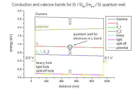
Strain is zero except for the exx, eyy and ezz
strain tensor components inside the Si0.7Ge0.3 quantum
well region. This leads to a splitting of the X conduction band. This
structure was grown pseudomorphically on Si. So the SiGe alloy is strained
pseudomorphically with respect to this Si substrate.
- We are interested in the eigenvalues (energies) and
eigenfunctions (Psi2) of the electrons in the L band
inside the quantum well. We can see that there are 5 bound states inside the
quantum well. (They are the same for both Neumann and Dirichlet boundary
conditions. However, delocalized states (here: (6)) differ for Neumann
and Dirichlet). The eigenenergies are given in eV and the electron wave
functions (squared) are plotted.
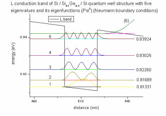
All this information is given in the file
Schroedinger_1band/cb002_qc001_sg001_deg001_neu_shift.dat
(L band, Neumann)
which contains the eigenvalues and Psi2. The suffix shift
indicates that the square of the wave functions is shifted by its
eigenvalue. Then the wave functions can be plotted much nicer into the band
edge plot.
The columns are ordered as follows:
position (nm) eigenvalue 1 (eV) ... eigenvalue 10 (eigenfunction 1)2 ... (eigenfunction 10)2
More information can be found in the file Schroedinger_1band/sg_info.txt
and in
$output-1-band-schroedinger
The band edge profile of the L conduction band profile was taken from the file
cb1D_L.dat.
- The Fermi levels for electrons (n) and holes
(p) of the Si / SiGe / Si quantum well structure (applied voltage 0.1
V):
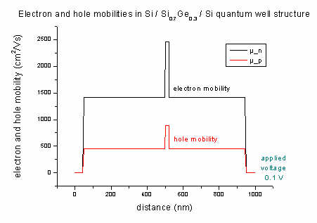
- The mobility of electrons and holes of the Si / SiGe / Si quantum well
structure (applied
voltage 0.1 V):
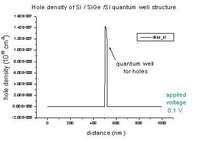
- The density of electrons and holes of the Si / SiGe
/ Si quantum well (applied voltage 0.1 V):
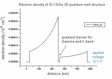
The Si0.7Ge0.3 alloy acts as a quantum well for heavy,
light and split-off holes
- Step 4: Read in data and solve k.p
Now we move on to
input_file4.in.
In the third file, we solved the current problem with 1-band Schrödinger and
saved the data (electrostatic potential and Fermi levels). Now we read in the
electrostatic potential and the Fermi levels again in
order to get the k.p wave functions. The input file has to remain
almost the same, just the quantum model is changed from effective-mass
to 6x6kp.
Also the flow-scheme
is now number 3 (read in raw data and calculate eigenstates).
So let's see if it works...
- Since we want to read in raw data and solve for eigenfunctions, we take
 flow-scheme
	= 3
which means that the built-in potential, the potential and the quasi Fermi
levels, which completely determine the system, will be read in. For this
potential, the specified eigenstates will then be calculated.
We have to specify from which directory the raw data has to be read in:
raw-directory-in = raw_data/
We also need to set the flags to yes to read in raw data:
  raw-potential-in    = yes


  raw-fermi-levels-in = yes
- Output k.p data
Possible outputs for k.p
Bulk k.p dispersion
- Plots dispersion of bulk k.p Hamiltonian including strain
effects.
- Filename: 'bulk_6x6kp_dispersion_000_kxkykz.dat'
See tutorial: k.p dispersion in bulk GaAs (strained / unstrained)
k|| dispersion
- Plots dispersion perpendicular to quantization axes for eigenvalues from
min to max.
- Result: 2D plot in
AVS/Express format.
- Data files for 1st subband: 'kpar1D_disp_00_10_hl_6x6kp_ev_001_2Dplot.dat
/ .coord / .fld'
Eigenvalues, eigenfunctions
- Filename: kp_6x6eigenvalues_qc001_kpar0001_Kz001_dir.dat
- Specifier:
kp_8x8, kp_6x6 |
kind of k.p solved |
_el, _hl |
electrons/holes |
eigenvalues, psi_squared |
eigenvalues, eigenfunctions squared |
_qc001 |
quantum cluster 1 |
_ev001 |
eigenvalue 1 |
_kpar001 |
number of k|| = 1 |
_Kz001 |
number of superlattice vector = 1 |
_dir, _neu |
boundary conditions Dirichlet or Neumann |
More information:
$output-kp-data
- Output
- The band structure will be saved into the directory band_structure/
- The densities will be saved into densities/
- The strain will be saved into strain/
- The current will be saved into current/
- Raw data will be saved into raw_data/
- k.p data will be saved into kp_data/
- Now run the executable and have a look at the output files.
This time the calculation takes more time (maybe even some minutes).
- In the k.p directory
kp_data/ you will find
for each eigenvalue 3 files:
- eigenvalue
position in space [nm], eigenvalue
- eigenfunction squared
position in space [nm], Psi2 (sum of components),
squares of components of k.p vector (8 in case of 8-band k.p / 6
for 6-band k.p)
In our case for 6-band k.p each file contains information about the
holes ordered in the basis
| x+ >, | y+ >, | z+ >, | x-
>, | y- >, | z- >| x >, | y >, | z > correspond to x, y, z of the calculation
system.
+ (spin
up) and - (spin
down) correspond to the spin projection along the z
axis of the crystal system.
Spin up and spin down eigenvalues are degenerate in this example.
Here we plot the energies and hole wave functions (squared) of our
6-band k.p
calculation. We have twofold spin degeneracy, thus we only plot spin up
values. The 9th eigenvalue (and of course also the 10th)
has light hole character whereas the first eight eigenvalues have heavy hole
character.
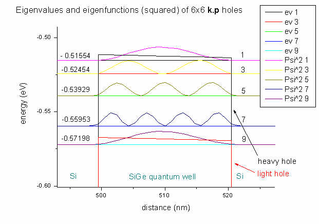
The arrows point to the heavy hole and light
hole band edges.
|